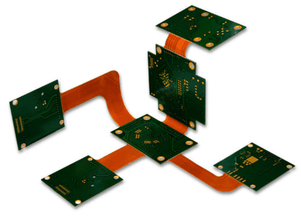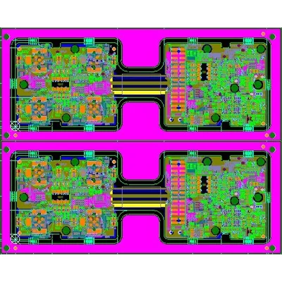
Rigid-Flex PCB Layout & Design
Name: Rigid-Flex PCB Layout & Design
Designable layers: 1-32 layers
Minimum line width and line spacing: 3mil
Minimum laser aperture: 4mil
Minimum mechanical aperture: 8mil
Copper foil thickness: 18-175цm (standard: 18цm35цm70цm)
Peel strength: 1.25N/mm
Minimum punching hole diameter: single side: 0.9mm/35mil
Minimum hole diameter: 0.25mm/10mil
Aperture tolerance: ≤φ0.8mm±0.05mm
Hole tolerance: ±0.05mm
Hole wall copper thickness: double-sided/multi-layer: ≥2um/0.8mil
Hole resistance: double-sided/multi-layer: ≤300цΩ
Minimum line width: 0.127mm/5mil
Minimum pitch: 0.127mm/5mil
Screen printing color: black, white, red, green, etc.
Surface treatment: lead/lead-free tin spray, ENIG, silver, OSP
Service: Provide OEM service
Certificate: ISO9001.ROSH.UL
One of the key features of rigid-flex PCBs is their thin profile and variable shapes, making them an ideal solution for ultra-thin and ultra-light packaging. Although rigid-flex boards can be more expensive to design and manufacture, they do offer many advantages and solve many of the problems with traditional rigid board technology.
1. Small size and flexible shape
Rigid-flex PCBs make it easier to fit more components in a smaller space because they can change shape according to specific contours. This technology will reduce the size and weight of the final product as well as the overall system cost. At the same time, the compact form factor of rigid-flex PCBs makes them the best choice for thin lines and high-density circuits in HDI technology.
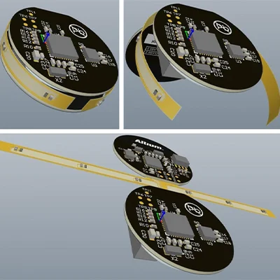
2. Can be customized for different applications
The package geometry freedom of rigid-flex PCBs can be customized for applications in many industries, including aerospace, military, medical devices, and consumer electronics. They can be customized in size and shape to suit housing designs and 3D designs, which gives designers more possibilities to meet different requirements in specific applications.
3. Better mechanical stability
The stability of the rigid board and the flexibility of the flexible board form a stable structure for the entire package, while retaining the reliability and flexibility of electrical connections required for installation in small spaces.
4. Better performance in harsh environments
Rigid-flex PCBs have high shock and vibration resistance, so they can work well in high stress environments. Fewer cables and connectors are used in rigid-flex PCBs, which also reduces safety risks and maintenance in future use.
5. Easy to manufacture and test
Rigid-flex PCBs require a lower number of interconnects and associated components/parts. It helps simplify assembly operations, making rigid-flex PCBs easier to assemble and test. Rigid-flex PCBs are great for PCB prototyping.
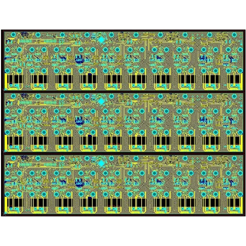
Name: Rigid-Flex PCB Layout & Design
Designable layers: 1-32 layers
Minimum line width and line spacing: 3mil
Minimum laser aperture: 4mil
Minimum mechanical aperture: 8mil
Copper foil thickness: 18-175цm (standard: 18цm35цm70цm)
Peel strength: 1.25N/mm
Minimum punching hole diameter: single side: 0.9mm/35mil
Minimum hole diameter: 0.25mm/10mil
Aperture tolerance: ≤φ0.8mm±0.05mm
Hole tolerance: ±0.05mm
Hole wall copper thickness: double-sided/multi-layer: ≥2um/0.8mil
Hole resistance: double-sided/multi-layer: ≤300цΩ
Minimum line width: 0.127mm/5mil
Minimum pitch: 0.127mm/5mil
Screen printing color: black, white, red, green, etc.
Surface treatment: lead/lead-free tin spray, ENIG, silver, OSP
Service: Provide OEM service
Certificate: ISO9001.ROSH.UL