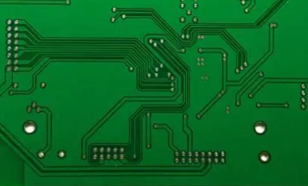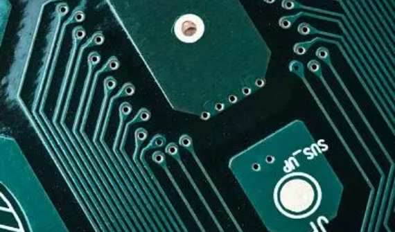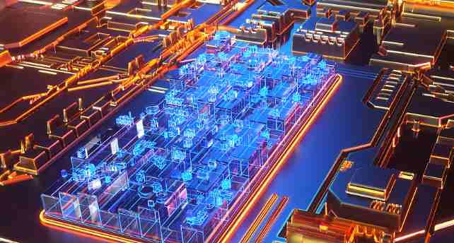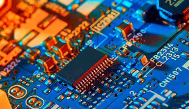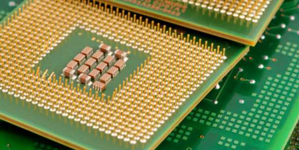
High - level circuit board key production process control
Due to the number of high-rise board layers, the customer design end of PCB layer alignment requirements are more and more strict, usually the inter-layer alignment tolerance control ±75μm, considering the large size design of high-rise board units, graph