
Professional PCB manufacturing and assembly
Building 6, Zone 3, Yuekang Road,Bao'an District, Shenzhen, China
+86-13410863085Mon.-Sat.08:00-20:00


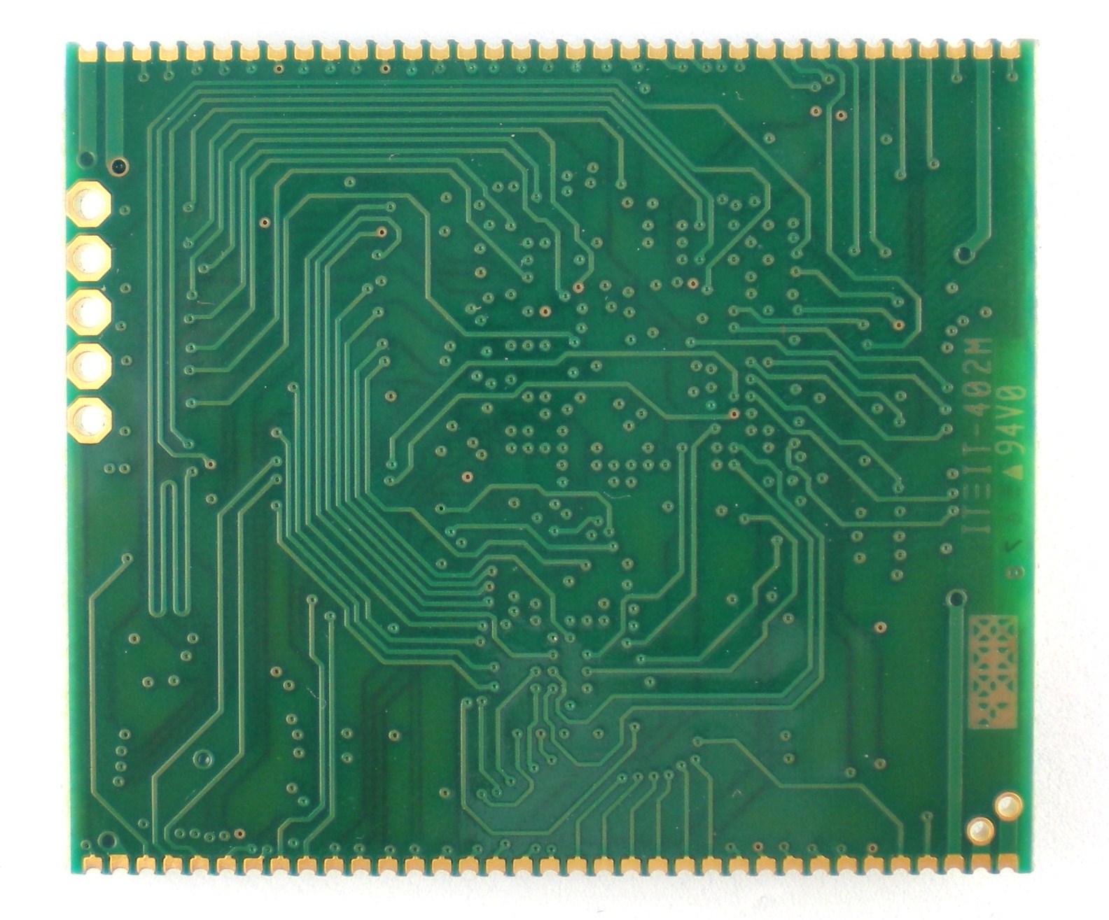
The circuit board is divided into three large categories according to the number of layers: single panel, double panel, and multi-layer circuit board. PCB is the English (Printed Circuit Board) printed PCB, short for circuit board. Usually on the insulation material, according to a predetermined design, made of printed lines, printed components or a combination of the conductive graphics called printed circuits. The conductive pattern that provides the electrical connection between the components on the insulating substrate is called the printed line. In this way, the printed circuit or printed circuit of the finished board is called printed circuit board, also known as printed board or printed circuit board.
The circuit board software designed by many circuit board designers is designed according to the components of the circuit board software itself, and the circuit board pad is not very large, so whether the circuit board pad is too small affects the circuit board welding?
Our common component welding methods are wave welding and tin pot welding, wave welding is through the wave welding machine to the circuit board welding, this welding method is not very high requirements for the welding pad of the circuit board, the welded circuit board is relatively orderly, and the tin pot welding has strict requirements for the welding pad of the circuit board, many circuit board welding factory thinks that the welding pad is too big to waste tin. In fact, the solder pot welding circuit board if the welding pad is too small will appear welding phenomenon, if there is a leak welding must use manual welding, that is a waste of labor, if the solder pot welding circuit board welding plate is large then it is not easy to appear welding phenomenon, compared to the latter although waste some tin but the overall working time and labor will save a lot. Therefore, it is recommended that the circuit board designer should increase the welding pad as much as possible to ensure high quality welding by keeping the circuit board and pad free from short circuit.
Amalfitano commented: "In general, flexible PCB circuits do cost more than rigid circuits and have always been more expensive. Relative to rigid plates, when flexible plates are manufactured, in many cases they have to face the fact that many parameters are out of tolerance. The difficulty in manufacturing flexible PCB circuits is the flexibility of the material. On the rigid plate, you are machining a 15mil FR-4 glass cloth plate, you put a hole in the glass cloth plate or do all the processing, and when you come back, that hole is still in the exact position. On flexible materials, when you come back, the hole has moved 5mil. That's the number one reason why flexible panels are expensive."
2.3 The cost of flexible PCB circuits is being further reduced
Despite the above cost factors, the price of flexible assembly is falling and becoming closer to that of traditional PCBS. This is mainly due to the introduction of newer materials, improved production processes and structural changes. There is an example where the use of acrylic adhesives has been eliminated on rigid-torsion plate assemblies with many layers. If you build a 12 - or 14-layer rigid-torsion PCB board and you use acrylic in it, you will have Z-axis expansion and metallization hole failure." Barry said, "The current structure makes the product more thermal stable and there are very few material mismatches. As output rises, costs come down. Newer materials now allow for finer lines due to thinner layers of copper. The thinner copper layer makes the components lighter and lighter, and the lighter and thinner assembly makes the flexible components better fit into smaller Spaces. In the past, we used a rolling process to adhere copper foil to a binder coated medium. Today, copper foils can be generated directly on the medium without the use of adhesives. These techniques can obtain layers of several microns of copper, allowing the industry to obtain fine lines of 3 mil or even narrower widths." After the adhesive is removed from the flexible PCB circuit, the flexible PCB circuit has flame retardant properties. This accelerates the UL certification process and further reduces costs. As flexible PCB circuits continue to evolve rapidly from their initial military industrial applications to civilian and consumer applications, achieving UL certification is even more important. Flexible plate solder masks and other surface coatings further reduce the cost of flexible assembly. Barry continues to believe that some of these new materials and processes have dramatically reduced costs over the past decade. At the same time, it is precisely because this type of product has been widely recognized and demand, the cost of flexible materials is also falling.
In the coming years, smaller, more complex and more expensive flexible PCB circuits will require more novel assembly and the addition of hybrid flexible PCB circuits. The challenge for the flexible PCB circuit industry is to strengthen its technological advantages and keep pace with computers, telecommunications, consumer demand and dynamic markets. In addition, flexible PCB circuits will play an important role in the lead-free action.
Hazards of not tracking exposure time
Jun 14,2023


Just upload Gerber files, BOM files and design files, and the KINGFORD team will provide a complete quotation within 24h.