
Professional PCB manufacturing and assembly
Building 6, Zone 3, Yuekang Road,Bao'an District, Shenzhen, China
+86-13410863085Mon.-Sat.08:00-20:00

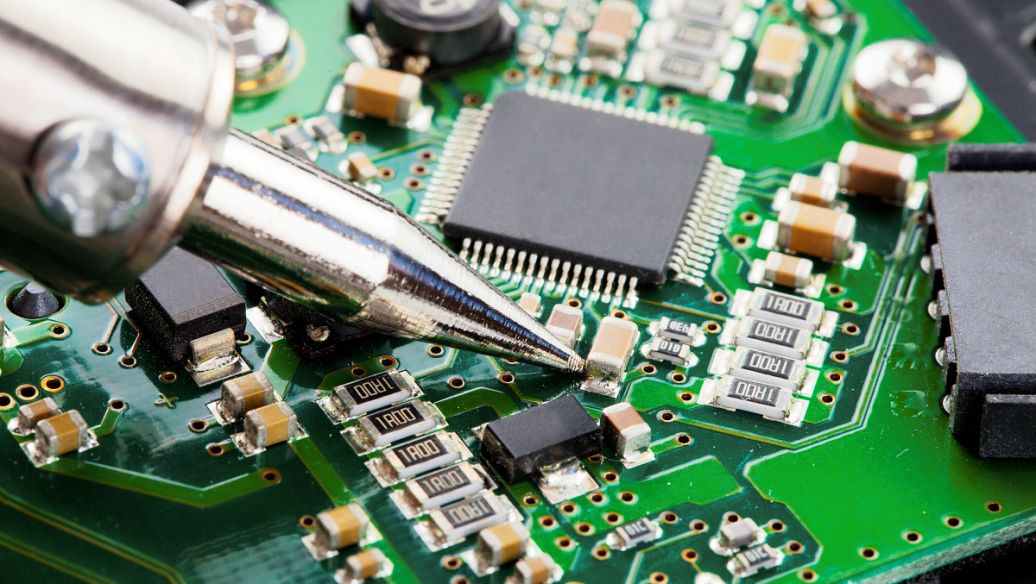
Proper PCB Assembly Process
Selecting the correct PCB assembly process is very important as this decision will directly affect the efficiency and cost of the manufacturing process as well as the quality and performance of the application.
PCB assembly typically uses one of two methods: surface mount technology or through-hole fabrication. Surface mount technology is the most widely used PCB component. Through-hole fabrication is rarely used, but is still very popular, especially in some industries.
Choosing a PCB assembly process depends on many factors. To help you make the right choice, we have compiled this short guide to choosing the right PCB assembly process.
PCB Assembly: Surface Mount Technology
Surface mount technology is the most commonly used PCB assembly process. It is used in many electronic products, from USB flash drives and smartphones to medical equipment and portable navigation systems.
This PCB assembly process allows the manufacture of products with increasingly smaller dimensions. If space is at a premium, then this is the one for you if your design has components like resistors, diodes, etc.
Surface mount technology allows for a higher degree of automation, meaning boards can be assembled faster. This enables you to process PCBs in high volumes and is more cost-effective than through-hole component placement. If you have unique requirements, surface mount technology can be highly customizable, so it's the right choice. If you need a custom designed PCB, this process is flexible and robust and can provide the desired results. Using surface mount technology, components can be mounted on both sides of the board. This double-sided board capability means you can implement more complex circuits without expanding the scope of your application.
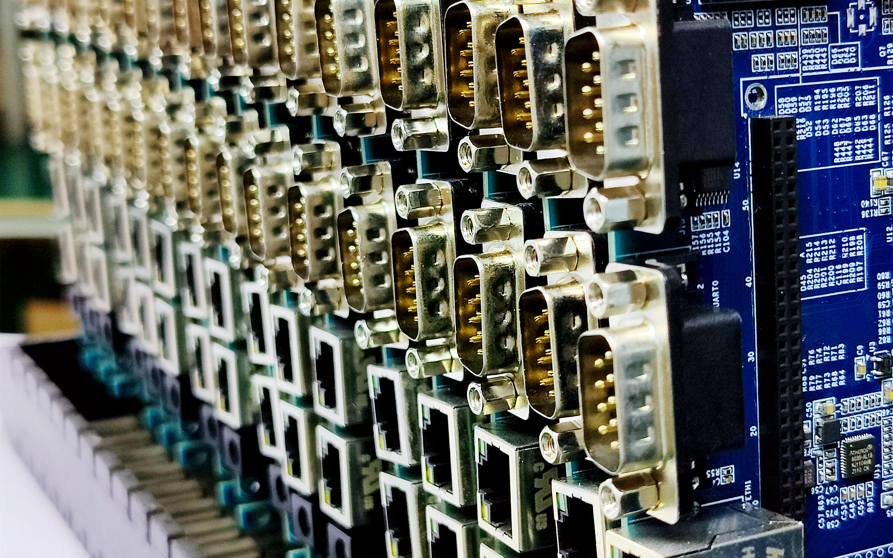
PCB Assembly: Through Hole Fabrication
Although through-hole fabrication is used less and less, it is still a common PCB assembly process.
PCB components fabricated using through-holes are used for large components such as transformers, semiconductors, and electrolytic capacitors, and provide a stronger bond between the board and the application.
Thus, through-hole fabrication provides a higher level of durability and reliability. This extra safety makes the process the preferred choice for applications in sectors such as the aerospace and military industries.
If your application must withstand high levels of stress (whether mechanical or environmental) during operation, then the best option for PCB assembly is through-hole fabrication. If your application must operate at high speeds and at the highest levels under these conditions, through-hole manufacturing may be the process for you. If your application must operate at high and low temperatures, the increased strength, durability, and reliability of through-hole fabrication may be the best choice for you. If it is necessary to operate at high voltage and maintain its performance, through-hole fabrication may be the best PCB assembly process for your application.
Additionally, due to continuous innovation and increased demand for increasingly complex electronics that require increasingly complex, integrated and smaller PCBs, your application may require two types of PCB assembly techniques. This process is called "hybrid technology".
Author: Quick Match PCB
Link: https://www.zhihu.com/question/479563337/answer/2123382586
Source: Zhihu
Copyright belongs to the author. For commercial reprint, please contact the author for authorization, for non-commercial reprint, please indicate the source.
Layer Lasagna or PCB
The next layer is thin copper foil. It is laminated to the circuit board with heat and adhesives. Typically, on a double-sided PCB, copper is applied to both sides of the substrate. In less expensive electronics, the PCB may only have copper on one side. When we say double-sided or double-layer board, we mean the number of copper layers in the lasagna.
This lasagna can be made with as few as 1 layer or as many as 16 or more layers.
The layer on top of the copper foil is called the solder mask. This layer gives the typical green color to the PCB. Apply it to the copper layer to insulate the copper traces. It eliminates the possibility of accidental contact with other metals, solder or conductive bits. This layer helps the user solder to precise locations and prevents solder skipping.
Apply a layer of white silkscreen on top of the solder mask. This silkscreen adds letters, numbers and symbols to the PCB. This allows for easier assembly and instructs humans to better understand the board. We often use silkscreen labels to indicate the function of each pin or LED.
A printed circuit board
Now back to our analogy:
On the top of the PCB, you can notice a series of lines running all over the place, connecting various components. Aren't our roads the same, with cities all over the place connecting all places? But here, instead of cars moving around, electrons are flying on copper roads, rushing to power one component after another! These copper tracks are called traces in our PCB city.
A city is where all major engineering takes place. We have offices, local businesses and more on every corner. This center of human activity is like those square black shapes found on PCBs called integrated circuits (ICs). These ICs are where all the hard work in the PCB takes place to do the quick calculations.
Suburbs are typical places for homes, parks and schools. From an airplane, you'll notice that suburban rows of houses often look like the little resistors you'd find on a PCB. These resistors significantly control charge flow through resistance.
No city is exempt from construction! Whether building a new skyscraper or a new apartment complex, you'll find new foundations everywhere. These bases are like empty pads without components that you find on PCBs. While they may be empty right now, a component will be soldered to them soon.
Even our PCB cities have their own street names and addresses.
< This form of addressing, called silkscreening, helps the person who assembles or fixes a PCB know exactly where and where a part is.
All the company water we use comes from local storage tanks, who find themselves traveling through pipes to different places. This system is like the holes you would find on a PCB, called vias. These help to get power from one side of the PCB to the other, much like our water goes from our local storage tank to our bathroom, it's a highway.
Power plants in cities keep their lights on. Can you imagine a city without them? Hope it's not zombie infested! Like power plants in cities, we put so-called capacitors on PCBs that store electricity. They hold the charge and release it when it needs to generate electricity.
Streetlights and signs help maintain order in a world full of crazy drivers. They control the flow of traffic on our labyrinthine streets and highways. On PCBs, diodes and their cousins LEDs are those signs and street lights. Diodes control the current flow on the PCB. It allows it to go in only one direction.
Common impedance pcb circuit boards
May 30,2023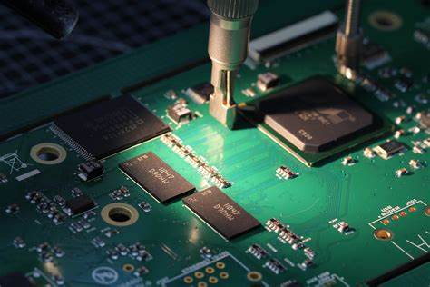


Just upload Gerber files, BOM files and design files, and the KINGFORD team will provide a complete quotation within 24h.