
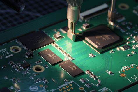
Professional PCB manufacturing and assembly
Building 6, Zone 3, Yuekang Road,Bao'an District, Shenzhen, China
+86-13410863085Mon.-Sat.08:00-20:00

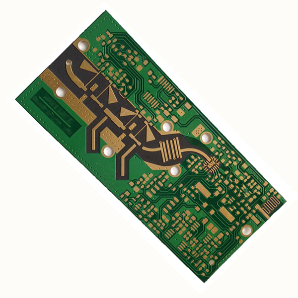
Common impedance pcb circuit boards
Definition of Impedance: In a circuit with resistance, inductance and capacitance, the hindrance to the current in the circuit is called impedance. Impedance is often represented by Z, which is a complex number. The real part is called resistance, and the imaginary part is called reactance. For inductive reactance, the blocking effect caused by capacitance and inductance on alternating current in the circuit is collectively called reactance. The unit of impedance is the ohm. The concept of impedance not only exists in the circuit, but is also involved in the vibration system of mechanics.
Classification of impedance: Common impedances are divided into three types: single-ended (line) impedance, differential (moving) impedance, and coplanar impedance.
Single-ended (line) impedance: English single ended impedance, refers to the impedance measured by a single signal line.
Differential (moving) impedance: English differential impedance, refers to the impedance measured in two equal-width and equal-spaced transmission lines during differential drive.
Coplanar impedance: English coplanar impedance, which refers to the signal line tested when it is transmitted between GND/VCC around it (the distance between the signal line and the GND/VCC on both sides is equal)
Impedance Influencing Factors:
The dielectric constant of the medium is inversely proportional to the impedance value, and the dielectric constant is calculated according to the newly provided "Plate Dielectric Constant Table".
H1, H2, H3...: The dielectric thickness between the line layer and the ground layer is proportional to the impedance value.
The width of the bottom of the impedance line; W2: the width of the impedance line, which is inversely proportional to the impedance.
A: When the inner bottom copper is HOZ, W1=W2+0.3mil; when the inner bottom copper is 1OZ, W1=W2+0.5mil; when the inner bottom copper is 2OZ, W1=W2+1.2mil.
B: When the bottom copper of the outer layer is HOZ, W1=W2+0.8mil; when the bottom copper of the outer layer is 1OZ, W1=W2+1.2mil; when the bottom copper of the outer layer is 2OZ, W1=W2+1.6mil.
C: W1 is the original impedance line width.
: Copper thickness, which is inversely proportional to the impedance value.
A: The inner layer is the substrate copper thickness, HOZ is calculated as 15UM; 1OZ is calculated as 30UM; 2OZ is calculated as 65UM.
B: The outer layer is copper foil thickness + copper plating thickness, which depends on the hole copper specification. When the bottom copper is HOZ and hole copper (average 20UM, minimum 18UM), surface copper is calculated as 45UM; hole copper (average 25UM, minimum 20UM), surface copper is calculated as 50UM; when the minimum single point of hole copper is 25UM, surface copper is calculated as 55UM.
C: When the base copper is 1OZ and the hole copper (average 20UM, minimum 18UM), the surface copper is calculated as 55UM; when the hole copper is (average 25UM, minimum 20UM), the surface copper is calculated as 60UM; when the minimum single point of hole copper is 25UM, Table copper is calculated by 65UM.
The spacing between adjacent lines and lines is proportional to the impedance value (differential impedance).
The thickness of the substrate solder mask is inversely proportional to the impedance value; C2: the thickness of the solder mask on the line surface is inversely proportional to the impedance value; C3: the thickness of the solder mask between the lines is inversely proportional to the impedance value; CEr: the dielectric constant of the solder mask is proportional to the impedance The value is inversely proportional to.
A: Print solder resist ink once, the value of C1 is 30UM, the value of C2 is 12UM, and the value of C3 is 30UM.
B: Solder resist ink is printed twice, the value of C1 is 60UM, the value of C2 is 25UM, and the value of C3 is 60UM. C: CEr: Calculated according to 3.4. In the transmission signal line of electronic devices, the resistance encountered when high-frequency signals or electromagnetic waves propagate is called impedance. Why do PCB boards have to do impedance in the manufacturing process? Let us analyze from the following 4 reasons:
1. The pcb circuit board should consider plugging and installing electronic components, and the later SMT patch plugging also needs to consider issues such as electrical conductivity and signal transmission performance, so the lower the impedance, the better.
2. In the production process of pcb circuit board, it has gone through manufacturing processes such as copper sinking, electroless tin plating (or chemical plating, thermal spray tin), connector soldering, etc. The materials used must require low resistivity in order to ensure the overall impedance value of the circuit board Only when the product quality requirements are met can it operate normally.
3. The tinning of PCB circuit board is the most prone to problems in the whole circuit board production, and it is the key link that affects the impedance; its biggest defect is easy oxidation or deliquescence, poor brazing performance, which makes the circuit board difficult to weld and the impedance is too high High, resulting in poor electrical conductivity or instability of the overall performance of the board. the
4. The conductors in the pcb circuit board will have various signal transmissions. The line itself will change the impedance value due to factors such as etching, laminate thickness, and wire width, which will distort the signal and cause the performance of the circuit board to decline. It is necessary to control the impedance value within a certain range.
Impedance matching technology:
input resistance
Input impedance is the equivalent impedance at the input of a circuit. Add a voltage source U to the input terminal, measure the current I at the input terminal, then the input impedance R is U/I. You can think of the input as the two ends of a resistor, and the resistance of this resistor is the input impedance. The input impedance is no different from an ordinary reactive element, which reflects the size of the resistance to the current. For a voltage-driven circuit, the larger the input impedance, the lighter the load on the voltage source, so it is easier to drive and will not affect the signal source; while for the current-driven circuit, the smaller the input impedance, the The lighter the load on the current source. Therefore, we can think of it this way: if it is driven by a voltage source, the larger the input impedance, the better; if it is driven by a current source, the smaller the impedance, the better (Note: only suitable for low-frequency circuits. In the circuit, the impedance matching problem should also be considered.) In addition, if the maximum output power is to be obtained, the impedance matching problem should also be considered.
output impedance
Regardless of the signal source or amplifier and power supply, there is a problem of output impedance. Output impedance is the internal resistance of a signal source. Originally, for an ideal voltage source (including power supply), the internal resistance should be 0, or the impedance of an ideal current source should be infinite. Output impedance requires the most special attention in circuit design.
But real voltage sources cannot do this. We often use an ideal voltage source in series with a resistor r to be equivalent to an actual voltage source. This resistor r in series with the ideal voltage source is the internal resistance of (signal source/amplifier output/power supply). When this voltage source supplies power to the load, there will be a current I flowing through the load, and a voltage drop of I×r will be generated on this resistance. This will lead to a drop in the output voltage of the power supply, thereby limiting the maximum output power (for why the maximum output power is limited, please see the question "Impedance Matching" later). Similarly, for an ideal current source, the output impedance should be infinite, but it is impossible in a real circuit.


Just upload Gerber files, BOM files and design files, and the KINGFORD team will provide a complete quotation within 24h.