
Professional PCB manufacturing and assembly
Building 6, Zone 3, Yuekang Road,Bao'an District, Shenzhen, China
+86-13410863085Mon.-Sat.08:00-20:00

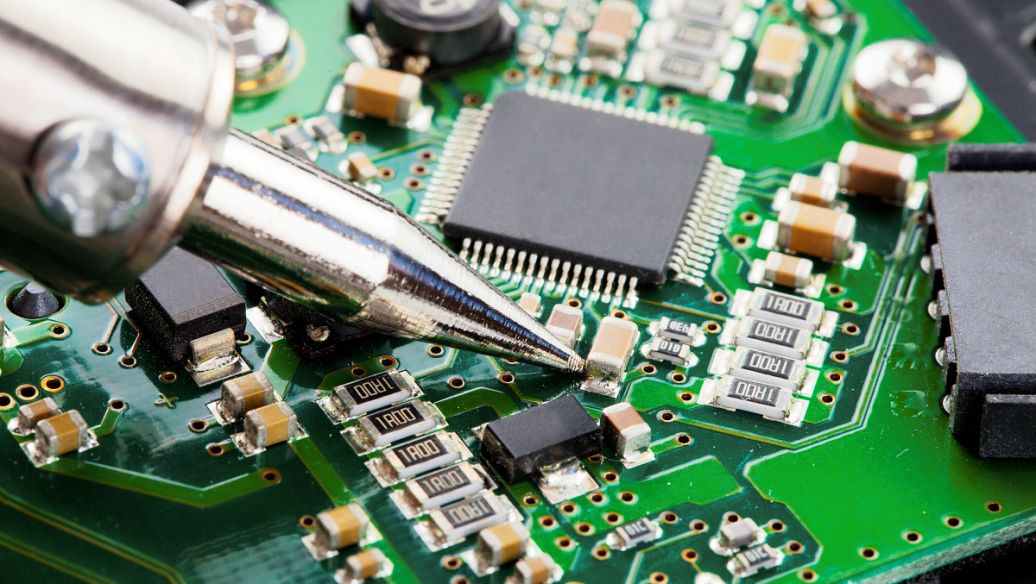
What should be paid attention to in small batch PCBA assembly
This is the process involved in PCBA production and assembly by reducing costs while ensuring high quality is maintained. Here, the processes employ various techniques to maintain quality and keep costs down.
Techniques used to secure low-volume PCBs
As mentioned earlier, the purpose here is to utilize unique technology in smt processing. This means you have to find some unique technique to help you assemble all the components of your PCB. Here are some techniques to use when assembling low-volume PCBs and still maintaining high quality.
Minimize the number of layers
This is a very important technique when it comes to reducing the costs associated with SMT assembly. This requires reducing the number of layers. In this way, the cost of components and materials will definitely be reduced
be careful when arranging
When assembling in the smt patch factory, care must be taken when arranging the number of vias. By doing so, errors of any kind will be eliminated or reduced, thereby reducing costs.
proper size
You must take extra care when adjusting and planning important details such as annular rings and holes. We mean it has to be perfect. When you keep your board size to a minimum, you should avoid mistakes
prevent internal cuts
Prevent internal cuts in printed circuit boards in smt patches. This will help eliminate the costs involved in repairing internal cuts. With this, you will be able to save on material costs for internal wiring as well as via drilling.
Choose the most suitable via
Selecting the most suitable vias, which does not cause any complication to the pcb assembly process, is very important here. Possibly buying vias at a higher price for this, but will save you a lot of money in the long run.
stick to the basics
Always stick to PCB assembly basics and don't risk a custom design. Keep the normal shape of the PCB and do not experiment with unusually shaped PCBs.
maintain industry standards
Make sure to keep to the standard requirements and don't venture into unknown territory. For this case, use only the correct standard components, dimensions and choose the correct finish.
Three Different Ways to Make a Blind Via PCB
1. Mechanically controlled depth drilling
In the traditional smt patch multilayer board manufacturing process, a drilling machine is used to set the Z-axis depth of the drilling, but there are some problems:
a. Only one can be drilled at a time, and the yield is very low.
b. The table of the drilling machine must be level, and the drilling depth of each spindle must be the same. Otherwise, it is difficult to control the depth of each hole.
c. Electroplating in the hole is difficult, especially when the depth is greater than the diameter of the hole, it is almost impossible to electroplate in the hole.
Due to the limitations of the process described above, this approach has become less popular.
2. sequential lamination
Take the 8-layer PCB board in smt patch processing as an example (see figure)
altium blind via
Sequential lamination in the smt chip factory can make blind holes and buried holes at the same time. First, make the circuit and PTH of the inner four layers (six layers + double layer, top layer double bottom layer, inner four layers). Then stack the four pieces into a four-layer board, and then punch holes. This method has a long technological process and high cost, and is not universal.
3. Forming process and non-mechanical drilling methods
This method is the most popular in the industry, and many domestic manufacturers have similar manufacturing experience.
This method extends the concept of sequential lamination above, adding layer by layer on the outside of the board, and using non-machined blind holes as interlayer interconnections. Here are the three main methods:
Photoresist - Photoresist is formed using photoresist, which is also a permanent dielectric layer. Then develop the exposed film at a specific position to expose the copper pad at the bottom to form a bowl-shaped blind hole. After etching, smt manufacturers can get external circuits and blind holes. Instead of copper plating, copper paste or silver paste is filled to complete conduction. According to the same principle, it can be added layer by layer.
Laser Ablation - There are three types: CO2 laser, excimer laser, Nd:YAG laser.
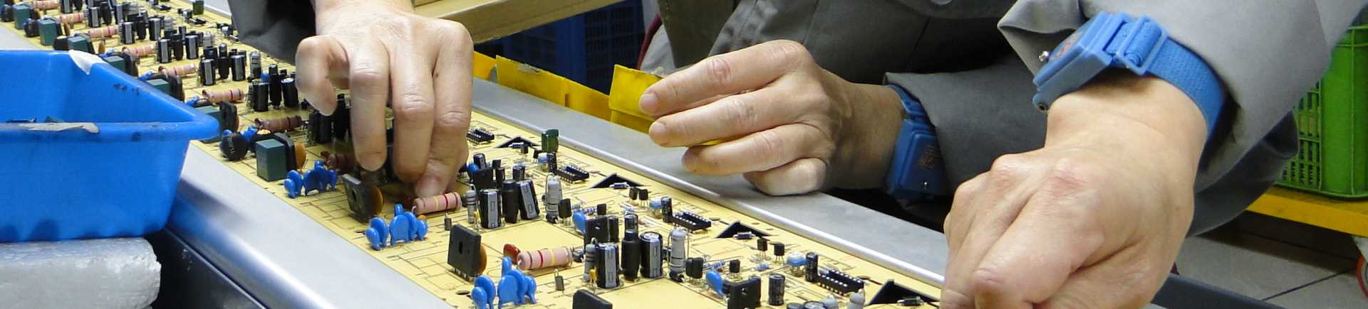
The impact of pcba small batch proofing and assembly on the overall cost Printed circuit boards, also known as printed circuit boards, printed circuit boards, often use the English abbreviation PCB, which is an important electronic component, a support for electronic components, and a circuit for electronic components The provider of the connection. Because it is made by electronic printing technology, it is called a printed circuit board. If we want to know where the cost is high in small batch proofing of pcba, we need to decompose the whole contracting of labor and materials. PCBA means PCB assembly, so it must include circuit board light board, component welding, smt surface mount and DIP These two parts are soldered after plug-in. At present, the price of bare boards on the market is between 350 and 550. The prices of components are basically open and transparent in major shopping malls, which can be compared for reference.
Since the main PCB circuit boards and components do not have the possibility of price increase in the dark, the cost level is reflected in the assembly process. The main costs of the assembly link are as follows:
1. SMT patch processing proofing, patch processing according to the number of points and packaging, there will be a certain difference in price. Large quantity and high price are the industry consensus. The larger the component package size, the easier it is to mount, and the corresponding poor quality will be reduced. Therefore, there is more room for communication in terms of price.

2. Welding hours after DIP plug-in, because the plug-in material link involves special-shaped parts and material forming, this link requires a lot of manual participation, because there is no production capacity reference of machinery and equipment, this link is the most difficult link to control the cost. At the same time, the current labor cost remains high, and the cost of this link is generally high.
3. Assembly test: test fixtures, test equipment, test man-hours, test fixtures currently range from tens to hundreds of yuan according to the difficulty of the test, and the test of communication equipment also requires the assistance of optical fiber, ICT and other test equipment, and the corresponding labor And equipment loss needs to be taken into account, but it will not be very high, and some companies even test for free.
4. Auxiliary materials: solder paste, tin bar, flux, UV glue, furnace fixture, the quality of solder paste and solder bar is the most important auxiliary material in the whole processing link. Generally, the price of domestic solder paste is 180~260 / bottle, imported solder paste may be 320~480 / bottle, so the price of imported solder paste will be much higher for the same soldering area, but the difference in soldering quality is very obvious.
Proper PCB Assembly Process
May 30,2023


Just upload Gerber files, BOM files and design files, and the KINGFORD team will provide a complete quotation within 24h.