
Professional PCB manufacturing and assembly
Building 6, Zone 3, Yuekang Road,Bao'an District, Shenzhen, China
+86-13410863085Mon.-Sat.08:00-20:00


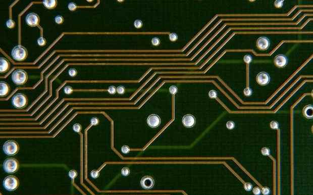
The wiring of PCB circuit board is a very important link, the wiring of PCB circuit board has the following principles:
1, all parallel signal lines should be as far as possible to leave a large interval to reduce crosstalk. If there are two signal cables close to each other on the pcb board, you are advised to route a ground cable between the two cables to shield them.
2, the design of signal transmission line to avoid sharp bends, in order to prevent the transmission line characteristic impedance mutation and reflection, to try to design into a certain size of uniform arc line.
3. If there is a small signal amplifier on the board, the weak signal line should be far away from the strong signal line before amplification, and the line should be as short as possible, and if possible, the ground line should be shielded.
4. If there are large current devices on the board, such as relays, indicators, horns, etc., their ground wires should be separated separately to reduce the noise on the ground wire. The ground wires of these large current devices should be connected to an independent ground bus on the plug-in board and backplane, and these independent ground wires should also be connected to the ground point of the entire system.
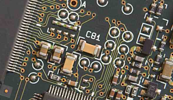
There are several PCB circuit board appearance processing methods
Often used PCB circuit board appearance processing methods are the following, PCB circuit board appearance processing can be based on the printed board appearance and processing quantity and different materials to choose processing methods, often used PCB circuit board appearance processing methods are the following:

This PCB circuit board shape processing method is the use of shearing machine for cutting processing can be used for blanking. Frame line as the basis of PCB circuit board contour processing, cutting processing can only be processed straight shape, special-shaped local available punch and milling machine processing. For the variety, the number is small, the size of the printed board is not high requirements often use this method for PCB circuit board appearance processing, the disadvantage is poor accuracy, sometimes also need sandpaper polishing.
The gap between punch and die can be reasonably designed according to the thickness and contour size of the printed board.
3 Milling machine processing of the PCB circuit board shape processing method is more flexible. The excess arc at the corner must be allowed to be greater than or equal to the minimum cutter radius. CNC milling machine can be processed printed board shape, because the milling cutter is cylindrical so in the design of printed board shape and special-shaped holes. High processing precision, can be processed various shapes, sizes of the board. Nc milling is suitable for large batch, complex shape, high precision requirements of printed board milling. The movement of the table or rotating shaft is automatically controlled by the sequence. The operator only needs to compile the sequence according to the outline size and load and unload the printed board to the CNC workbench.
4.4 Ensure the repetition accuracy of the device
When the solder paste is printed, due to the offset between the steel mesh and the solder pad, if the offset is too large, it will lead to the solder paste dipping to the outside of the solder pad, and the tin bead is easy to appear after heating. The precision of the patch also affects the manufacturing process. Generally speaking, more than three sigma will suffice. Otherwise, the probability of tin beads will be increased.
4.5 Control the pressure of the patch machine
There are two ways for the height of Z-axis when the mounter pastes components, one is the pressure control, the other is the thickness control. The height of the Z axis determines how much the element presses down on the solder paste. This is also an important factor causing tin beads. The pressure of the solder paste is not well controlled, and the solder paste will be extruded to the outside of the solder plate when the component is attached, which will cause tin beads. Therefore, whether it is attached pressure control mode, or component thickness control, need to adjust the setting to prevent tin beads.
The pressure is controlled by the principle of just being able to "place" the element on the solder paste and press down to the appropriate height, which is not able to squeeze the solder paste out of the pad. Different suppliers, models, packaging components need different control pressure, to pay attention to the production, when necessary to adjust the pressure.
4.6 Optimize the temperature curve
In the four stages of reflow welding, the preheating and holding stages aim to reduce the thermal shock of PWB and components and ensure that the solvent of solder paste can partially volatilize during the action, so as to avoid collapse or spatter caused by too much solvent due to the rapid rise of temperature in reflow welding, and the solder paste rushes out of the pad and forms tin beads or tin balls.
The solution is to control the temperature of reflow welding. Ensure that the heating rate of the preheating zone is in a moderate position below 2°C/S, and the time of the insulation zone is controlled within 60-120s, so that most of the solvent can volatilization on a better platform.
5 Closing Remarks
There are many reasons for tin beads. In this regard, our company first prevents tin beads in the design of steel mesh.
SMT production process control is multifaceted, any aspect is not done well, there may be problems. Therefore, in addition to the attention of SMT technicians, departments related to purchasing and material control also need to actively cooperate with SMT technicians. They should consider communicating with the technicians about material changes and replacements, so as to prevent the defects caused by changes in process parameters caused by material changes. Designers responsible for PCB circuit design should also communicate more with craftspeople, and the improvement suggestions put forward by craftspeople should be referred to and improved as far as possible. Only with the cooperation of various aspects can SMT problems be improved well.


Just upload Gerber files, BOM files and design files, and the KINGFORD team will provide a complete quotation within 24h.