
Professional PCB manufacturing and assembly
Building 6, Zone 3, Yuekang Road,Bao'an District, Shenzhen, China
+86-13410863085Mon.-Sat.08:00-20:00

According to IPC-7525A steel mesh design standard, the correct choice of steel sheet thickness, strictly control the opening proportion of laser steel mesh. When selecting the thickness of steel sheet, under the condition that the quality of solder joint is guaranteed, the lower thickness shall be selected according to the standard of IPC-7525A and the actual PCB components, and the larger one shall be avoided as far as possible. For example, according to the standard, 0.125mm -- 0.15mm thickness of steel sheet can be selected for QFP/Pin0.5mm spacing, but in actual production, if the selection of 0.12mm steel sheet does not affect the welding effect of other components, it should be selected 0.12mm rather than other larger.

The opening ratio is generally 1:1, but for some components with large demand for solder paste, the opening ratio can be appropriately increased to 1:1.05 or 1.2. However, for SMT steel mesh with opening ratio greater than 1:1, it is necessary to pay attention to the frequent and effective cleaning of its bottom in printing, otherwise it will also cause tin balls because of the accumulation of solder paste at the bottom. For some parts with relatively small solder paste demand, the opening ratio can be appropriately reduced to 1:0.9. Among the chip components, less than 0402 can not open the tin bead hole, and above 0603 need to open the tin bead hole selectively.
At the same time, according to the reason that the tin bead is related to the tin paste in the inner extension part of the pan, the inner extension part of the pan can be canceled, or even the inner extension part of the pan is designed as a negative value.
4.2 Select the appropriate welding pad graphics and size design
Poor dimensional design of the pad can also lead to tin beads. In the actual pad design, should be combined with IPC, according to the actual component package size, welding end size, to design the corresponding pad size. Each company should develop a design standard suitable for manufacturing pads based on the size of components presented by its own suppliers. At the same time, the design should be modified according to the actual situation.
According to IPC-SM-782A, the solder joint has three reference values:
Jt = Solder fillet attoe, solder fillet attoe
Jh = Solder fillet atheel, solder fillet atheel
Js = Solder fillet atside, solder fillet atside
The following is the basic design of our welding pad.
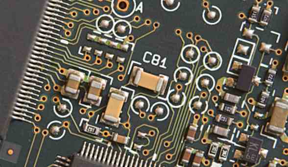
For chip components, take 0402 components as an example. Figure 3 is the schematic diagram of resistance pad design (actual graphics vary with components, and are listed here separately), and Figure 4 is the schematic diagram of corresponding resistance component size (bottom). FUJI 143E high speed SMT machine was used for measurement with accuracy of 0.001mm. The size of PCB pad actually measured is shown in Table 1. The comparison between the component size based on actual measurement (FUJI143E patch measurement, accuracy 0.001mm) and that provided by the supplier is shown in Table 2. The dimensioned data of the actual measurement and the dimensioned data provided by the supplier are within the specified range. Three reference values
The calculation formula is as follows:
Jt is equal to Z minus L over 2
Jh = (S-G) /2
Js = (X minus W) /2
If the Jh value is positive, it means that there is no surplus solder paste at the welding end after installation, so that a part of the solder paste will be "redundant". If the Jh value is positive and the value is relatively large, the temperature rise rate during welding is too fast, the solder on the welding end or pad is poor, the mounting pressure is too large and other factors may cause tin beads. If the value is positive but small, it will make for a good fillet.
According to the IPC-SM-782A standard, the actual Jh is:
Resistance Jh = (0.46-0.4) /2=0.03mm
Capacitance Jh= (0.66-0.4) /2=0.08mm
Although both Jh values are positive, they are relatively small, so that the solder paste can form a good soldering peak and wetting Angle at the root without forming tin beads. The actual situation is rarely found tin beads, the actual welding condition is also very good. The empirical value of Jh is a good range of -0.1 -- 0.15mm. The range of S values in Table 2 is very large. In practice, the manufacturer can be required to control the range, and the capacitor and resistance should be within 0.35-0.65mm. Otherwise change the steel mesh design to suit.
The rest of the Jt, Js case can be analogized.
The IC component can be designed according to the graphics (or even size) provided by the supplier. The chip component category is currently recommended by the industry lead-free pad is extroverted semi-elliptical or introverted semi-elliptical type can be. As long as the consideration is to avoid the past square pad prone to stress concentration and mounting pressure will overflow solder paste in the corner and form tin beads.
4.3 Improve the cleaning quality of SMT steel mesh
Improving the cleaning quality of SMT steel mesh can improve the printing quality. If the cleaning is not clean, the residual solder paste at the bottom of the opening of the SMT steel mesh will gather near the opening of the SMT steel mesh to form too much solder paste and cause tin beads. Printing press in the choice of automatic cleaning of steel mesh is best to use wet cleaning, dry cleaning and vacuum three ways together, can make the cleaning effect is improved. The cleaning frequency can be appropriately increased according to the component layout of the product. Use also need to see whether the actual effect is good, otherwise also need to increase artificial scrubbing.
What are the PCB circuit board wiring principles
May 25,2023


Just upload Gerber files, BOM files and design files, and the KINGFORD team will provide a complete quotation within 24h.