
Professional PCB manufacturing and assembly
Building 6, Zone 3, Yuekang Road,Bao'an District, Shenzhen, China
+86-13410863085Mon.-Sat.08:00-20:00

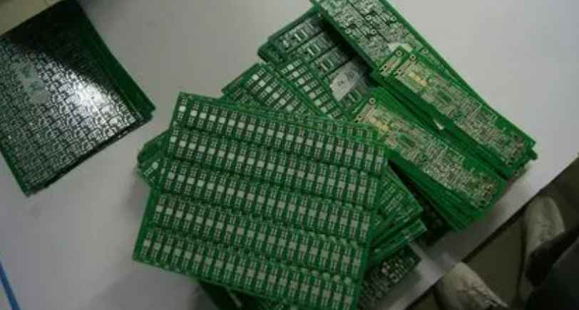
One of the most common physical repairs on PCBS 1 (restoring functionality to a defective PCB but not conforming to original specifications) is solder resistance film repair. The purpose of the solder shield is to prevent solder from flowing from one point to another during the initial assembly process. Damage to the solder shield (FIG. 1) may be cosmetic or functional in nature, for example, a solder shield that prevents solder from flowing down from the BGA to the "dog bone" type leads to a situation where the BGA ball solder joint is "inadequate" and in turn leads to defects.
Solder mask issues: Solder mask issues
There are several ways to damage the solder shield. Loss of solder resistance film may occur due to the breakdown of adhesion between the solder resistance film and PCB. The solder mask may also be damaged when uncontrolled heat sources and solder braid strips are used to remove solder from pad locations, such as scraping the solder mask off. If the solder mask is exposed to multiple thermal cycles, the solder mask may become brittle and crack. Poor adhesion to the solder mask may cause solder to short circuit, other welding abnormalities, or cause the solder mask to flow down the dog bone from the BGA pad.

There are several different techniques that can be used to repair solder mask, each with its own advantages and disadvantages. One method outlined in Section 2.4.1 of IPC-7721 is the use of a liquid solder mask. It can spread to areas in need of repair. The alternative mask is then cured by heat or ultraviolet light. After reading the manufacturer's instructions, selectively apply the UV-curable solder mask and place it under the correct wavelength UV lamp. Based on the output of the UV lamp (which can be measured using a radiometer), the curing time of the given solder resistance film, and the distance between the lamp and the solder resistance film, the maintenance technician can record the controlled procedure.
Another method is a simple technique of "spot" welding mask repair by using a repair "pen" (IPC 7721 2.4.1), usually cured by air drying or baking cycles. The liquid seeps out of the soft nib and can then be air-cured or heat-cured. Relative to the size of the modern BGA pad, the nib itself is very large, so it is a challenge to accurately apply the welding film material. Due to the porous nature of the dot coating head, it tends to collect debris (including flux residue, residual masks, and cleaners) from the circuit board. This absorbed debris can then re-contaminate other areas of the board. Personnel using this technique to repair solder mask require an advanced skill level, but even so, often do not have the skill to repair the appearance of solder mask compared to the method outlined in 2.4.1 in IPC-7721.
In addition to this pen repair method, there is another technique that uses polyimide, adhesive-supported in situ mesh plates to repair the solder mask underneath the BGA. This is a reliable method of placing BGA while servicing the solder shield. The advantage of this mesh is that it is easy to place the BGA while also providing isolation between pads and preventing short circuits between I/O. This method can be used to fix the support height between the BGA base and the PCB to control the collapse height, and also as a solder resistance film "auxiliary tape". When installed in place, the mesh acts like a solder mask repair template. This allows even technicians who are just starting the repair job to repair the damaged solder mask underneath the BGA.
Finally, there are welding resistance film repair screen technology. This method can save maintenance time when large area solder mask needs to be repaired. Ultra-thin mesh can define the area of solder resistance film required for maintenance. The replacement solder film material is scraped into the mesh holes and then cured. After curing, the mesh is stripped, leaving a hardened replacement solder mask in its path. While this method can save time for multiple boards that need to be repaired in exactly the same area or for very complex large area repairs, it requires a service technician with an advanced skill level.
There has been little innovation in the display industry since leds replaced CFL tubes as the main backlight for LCDS. However, this is changing as backlight modules increasingly feature Mini leds, which offer contrast comparable to OLED.
Mini leds show promise for new types of displays, such as LED-based video walls, allowing large-area displays to far outperform previous technologies.
The most difficult part of using Mini leds is assembling and soldering them onto the PCB. A typical Mini LED has an edge length of 240 µl or less. The weld points that can accommodate these tiny components are smaller.
Solder paste printing verification
Steel mesh printing is still the primary method of tinning for Mini LED applications, but small stencil apertures are required at these size levels. In order to print very small solder paste uniformly and reliably on the circuit board, the solder paste must have a particle diameter of less than 15 µl. The steel mesh must be manufactured with the highest precision.
Solder paste can only be printed effectively if the press can provide accurate alignment and the printing head can distribute the finest structure. In order to reliably detect and verify this small geometry, an accurate and integrated detection device is needed.
As with all PCB repairs, prior notice must be given to the customer if the solder mask needs to be repaired while the PCB is being serviced. There are several repair methods that are specific to the purpose of assembly, cost, and complexity of the solder mask required to be repaired.
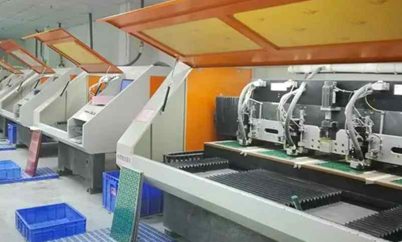
PCBA processing process
Mar 13,2023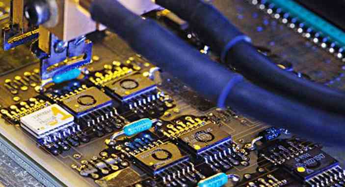


Just upload Gerber files, BOM files and design files, and the KINGFORD team will provide a complete quotation within 24h.