
Professional PCB manufacturing and assembly
Building 6, Zone 3, Yuekang Road,Bao'an District, Shenzhen, China
+86-13410863085Mon.-Sat.08:00-20:00

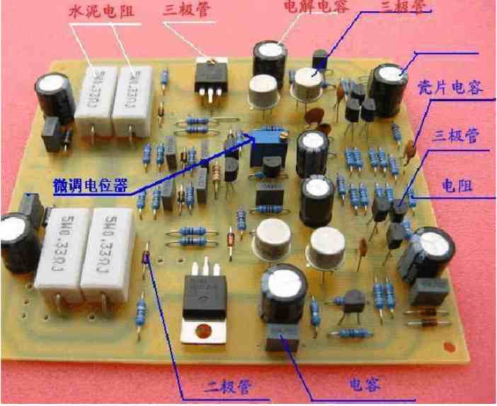
The thickness of double-sided circuit board copper foil is very important for the whole electronic products. Different products have different thickness requirements for circuit board copper foil. Some low current electronic products can use some copper foil relatively thin circuit board, and high current electronic products can use copper foil relatively thick circuit board. So once the use of electronic products will make the circuit board line can not withstand so much current, which will lead to line burn and serious will lead to component burn.
Therefore, when processing double-sided circuit board, we should first choose the thickness of the copper foil used in our common circuit board among the most common copper foil 18um, 25um, 35um, 50um and 70um, of course, not the same as the circuit board copper foil gap is not the same as the international board, International plate belongs to the national standard circuit board copper foil thickness is only 35um, 50um and 70um thick copper foil is required to sink copper or chemical treatment to thicket the thickness of copper foil.
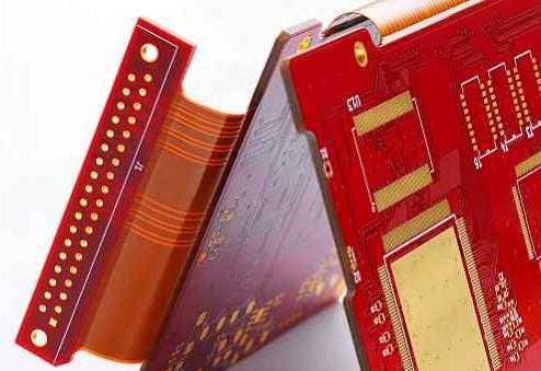
Talk about the application of soft and hard combined board and its advantages and disadvantages!
A brief description:
The birth and development of FPC and PCB gave birth to the new product of the combination of soft and hard board. Therefore, the combination of soft and hard board, is flexible circuit board and hard circuit board, after pressing and other processes, according to the relevant process
To combine together to form a circuit board with FPC characteristics and PCB characteristics.
Production process:
Because the soft and hard combined board is the combination of FPC and PCB, the production of soft and hard combined board should be equipped with both FPC production equipment and PCB production equipment. First, the electronic engineer draws the flexible bonding plate according to the requirements
The line and shape, and then, issued to the production of hard and soft combined board factory, after CAM engineers to the relevant documents for processing, planning, and then arrange FPC production line production required FPC, PCB production
PCB is produced online. After these two soft boards and hard boards are produced, the FPC and PCB are pressed together seamlessly by the press according to the planning requirements of the electronic engineer. After a series of details, the final process is completed
Soft and hard combined board. A very important link, should be the combination of hard and soft board is difficult, more details, before shipping, generally have to carry out a full inspection, because its value is relatively high, so as not to let the supply and demand sides
Resulting in the loss of relevant interests.
Advantages and disadvantages:
Advantages: The combination of soft and hard board has the characteristics of both FPC and PCB. Therefore, it can be used in some products with special requirements, with both a certain flexible area and a certain rigid area
Domain, to save the internal space of products, reduce the volume of finished products, improve product performance has a great help.
Disadvantages: the combination of soft and hard board production process is many, the production is difficult, the rate of good products is low, the material, manpower is more, therefore, the price is more expensive, the production cycle is longer.
Related fields of application:
The characteristics of soft and hard combined board determine its application field covering all the application fields of FPC in PCB, such as:
Mobile phone
Press the key plate and side keys
Computers and LCD screens
Motherboard and display screen
CD Walkman
Diskette drive
NOTEBOOK.
Latest use
hard disk drive (HDD,hard disk drive) mount circuit (Su print ensi. n cireuit) and xe packaging board, etc
How to remove the solder paste mistakenly printed on the PCB circuit board?
Expert teaches you how to remove the solder paste mistakenly printed on the PCB circuit board!
Answer: Using a small scraper to remove solder paste from misprinted plates can cause problems. It is generally possible to dip the misprinted plate in a compatible solvent, such as water with an additive, and then remove the small tin beads from the plate with a soft brush. Prefer repeated soaking and washing, rather than violent dry brushing or scraping. After paste printing, the longer the operator waits to clean the misprint, the more difficult it is to remove the paste. Misprinted plates should be placed in a soaking solvent as soon as the problem is discovered, as the solder paste is easily removed before drying.

Avoid using strips of cloth to wipe to prevent solder paste and other contaminants from coating the surface of the board. After soaking, a gentle spray can often help remove unwanted tin. Hot air drying is also recommended. If a horizontal template cleaner is used, the face to be cleaned should face down to allow the solder paste to fall off the board.
As usual, attention to a few details can eliminate undesirable situations, such as solder paste misprinting and removal from the board to solidified solder paste. The goal is to deposit the right amount of paste in the desired location. Soiled tools, dried solder paste, and misalignment of stencil and plate can result in unwanted solder paste on the underside of the stencil or even on the assembly. During the printing process, the stencil is wiped regularly between printing cycles. Ensure that the stencil sits on the pad and not on the solder shield to ensure a clean solder paste printing process. On-line, real-time solder paste inspection and pre-reflow inspection after component placement are all process steps that help reduce process defects before welding occurs.
For fine-pitch formwork, if damage is caused between pins due to the thin stencil cross-section bending, it can cause solder paste to deposit between pins, resulting in printing defects and/or short circuits. Low viscosity solder paste may also cause printing defects. For example, a high press temperature or a high scraper speed can reduce the stickiness of solder paste in use, resulting in printing defects and bridging due to excessive solder paste deposition.
In general, lack of adequate material control, solder paste deposition method and equipment are the main reasons for defects in reflow welding process.


Just upload Gerber files, BOM files and design files, and the KINGFORD team will provide a complete quotation within 24h.