
Professional PCB manufacturing and assembly
Building 6, Zone 3, Yuekang Road,Bao'an District, Shenzhen, China
+86-13410863085Mon.-Sat.08:00-20:00

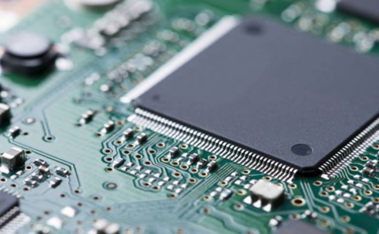
Nowadays, the PCBA processing and assembly of the circuit board basically solder the electronic parts onto the printed circuit board by solder. This welding process can be achieved through SMT, Surface Mount Technology or Wave soldering. Of course, you could hand weld all of them, but that's beyond the scope of this article, and hand welding is too risky to mass produce.
Because wave soldering has almost no products in use, so this article only introduces the surface welding (SMT) for circuit board assembly welding. Basically, the SMT manufacturing process now is a one-piece operation, that is, the empty board is put on the SMT production line, and the board is finally discharged and assembled in the same production line.
The following process will briefly describe the process from empty board loading to board assembly completion, as well as the quality assurance post process:
Empty plate loading
The first step of the assembly of the circuit board is to arrange the empty boards neatly, and then put them on the material rack. The machine will automatically send the boards into the SMT production line one by one.
Printing paste
The first step for the PCB to enter the SMT production line is to print the solder paste, which is really a bit like a girl applying a mask on her face. The solder paste is printed on the welding pad where the parts need to be welded. The solder paste will melt and be welded to the electrical parts on the board when it goes through the high-temperature back welding furnace.
Solder paste tester
Because the solder paste printing is related to the welding quality of the following parts, some SMT factories will use optical instruments to check the solder paste printing quality after the solder paste printing. If there is a bad printing board, the solder paste will be knocked off, the solder paste will be washed off and reprinted, or the excess solder paste will be removed by repairing.
Quick patch machine
Here, some small electronic parts (such as small resistance, capacitance, inductance) will be hit on the circuit board. These parts will be slightly stuck by the tin paste just printed on the circuit board. So even if the speed of the patch is very fast, almost like a machine gun, the parts on the board will not fly away, but large parts are not suitable for use in the fast machine. One will drag the speed of the small parts that were originally played very fast, and the other is afraid that the parts will offset the original position because the board moves quickly.
Universal type patch machine
Also known as "slow machine", here will be a number of large volume of electronic parts, such as BGA IC, connector... Etc., these parts need to be more accurate position, so alignment is very important, before the patch will first use the camera to confirm the position of the parts, so the speed is much slower. Because of the size of the parts here, they may not always have coil packaging, some may be tray or tubular packaging. However, an additional machine is required to enable SMT machines to eat pallets or tubes of packaging material.
Generally, the traditional patch/paste machine uses the principle of suction to move the electronic parts, so the top of these electronic parts must have a plane for the mouthpiece of the patch machine to absorb the parts, but some electronic parts can not have a plane for these machines, at this time, it is necessary to tailor special suction nozzle for these special-shaped parts. Or add a layer of flat tape to the parts, or wear a flat cap.
Patch processing
Hand swing parts or visual inspection
When all parts are printed on the printed board before going through the reflow furnace, a checkpoint is usually set up to pick out patch offset or missing parts... And so on the shortcomings, because after the high temperature furnace if there is still a problem must be moved to the iron, it will affect the quality of the product, there will be additional costs; Other large electronic parts or conventional parts of DIP or parts that for some special reason cannot be operated by the patch/paste machine will also be manually waved here.
In addition, an AOI will be designed for SMT of some mobile phone plates in front of the back welding furnace to confirm the quality before the back welding. Sometimes, the shielding frame will be placed on the parts, which will make it impossible to use AOI to check the solderability after the back welding furnace.
Backweld furnace
The purpose of the backwelding furnace is to melt the solder paste and form a total gold (IMC) in the parts foot and circuit board, that is, to weld the electronic parts on the circuit board, the curve of the temperature rise and fall will often affect the quality of the entire circuit board welding, according to the characteristics of the solder, the general backwelding furnace will set the preheating area, infiltration area, back welding area, cooling area, At present, the melting point of SAC305 solder paste without lead process is about 217℃, that is to say, the temperature of the backwelding furnace should be higher than this temperature at least to remelt the solder paste, in addition, the highest temperature should not exceed 250℃, otherwise many parts will be deformed or melted because they cannot withstand such a high temperature.
Basically, after the circuit board through the welding furnace, the assembly of the entire circuit board is completed, if there are hand welding parts exception, the rest is to check and test the circuit board has no defects or poor function.
Optical check for solderability
Not every SMT production line has an optical inspection machine (AOI). The purpose of AOI is to replace some circuit boards that are too dense for subsequent on-off and short-circuit electronic testing (ICT). However, AOI has its blind spots for optical interpretation, for example, the solder under parts cannot be judged. Currently, we can only check the parts for tombstone or side stand, missing parts, displacement, polarity direction, tin bridge and air welding, but we cannot judge the parts quality such as false welding, BGA weldability, resistance value, capacitance value and inductance value. So far, we cannot completely replace ICT.
Therefore, if only AOI is used to replace ICT, there is still some risk in quality, but ICT is not 100%. It can only be said that the test coverage rate can compensate each other, and we hope to achieve 100%, so we have to make a choice.
Folding plate
Once assembled, the boards are retracted to the racks, which have been designed to allow the SMT machine to automatically remove and remove the boards without compromising their quality.
Finished item inspection
No matter whether there is an AOI station or not, the general SMT line will still set up a visual inspection area for the circuit board. The purpose is to check whether there is any defect after the assembly of the circuit board. If there is an AOI station, the number of visual inspection personnel can be reduced, because it is still necessary to check some places where AOI cannot be interpreted, or check the defects of AOI.
Many factories will provide visual inspection templates at this station to facilitate visual inspection personnel to check some key parts and parts polarity.
Reassembly of parts
If some parts cannot be mounted with SMT, the parts will need to be hand-welded after the finished product inspection to distinguish whether the defect is from SMT or later in the process.
After the parts to use the soldering iron (iron) and tin wire, welding will maintain at a certain high temperature of the soldering iron contact with the feet of the parts to solder, until the temperature rises enough to melt the tin wire, and then add the tin wire melting, tin wire cooling will be welded on the circuit board parts.
When welding parts by hand, there will be some smoke, which will contain many heavy metals, so the operation area must be set up smoke discharge equipment, and try not to let the operator inhale these harmful fumes.
Need to remind, some parts will be due to the needs of the process and arranged in the later section of the process.
PCB circuit board open/short circuit test
The purpose of ICT setup is mainly to test whether the parts and circuits on the circuit board are open and short circuit. It can also measure the basic characteristics of most parts, such as the value of resistance, capacitance and inductance, so as to judge whether the functions of these parts are damaged, wrong or missing after the high temperature backwelding furnace. Etc.
Circuit testing machines are divided into advanced and primary testing machines. The primary testing machine is commonly referred to as MDA(Manufacturing Defect Analyzer), whose function is to measure the basic characteristics of electronic parts mentioned above and determine the opening and short circuit.
In addition to containing all the functions of the first stage of the test machine, the high level test machine can also be powered to the board to be tested, and start the board to be tested and execute the test program. The advantage is that the circuit board can be simulated in the actual startup of the functional test, can partially replace the following functional test machine. But a test fixture of this high level test machine can probably buy a private car, compared with a test fixture of the first level is 15~25 times higher, so it is generally used in the mass production of products.
Circuit board function test
PCBA functional test
Functional testing is to make up for the deficiency of ICT, because ICT only tests the on-off short circuit on the circuit board, and other functions such as BGA and products have not been tested, so it is necessary to use a functional testing machine to test all functions on the circuit board.
Cutting plate
General circuit boards will be assembled to increase the efficiency of SMT production, usually there will be so-called "several in one" board, such as two in one, four in one... Etc. Once all the assembly work is done, the board is cut into a single board, and some boards with only one board need to be cut off some of the excess edges.
There are several ways to cut the circuit board, you can design V-cut using blade cutting machine or directly manual folding plate (not recommended), more precise circuit board will use the path of the plate cutting machine, will not hurt the electronic parts and circuit board, but the cost and time is longer.
The knack of making circuit boards quickly
Mar 01,2023


Just upload Gerber files, BOM files and design files, and the KINGFORD team will provide a complete quotation within 24h.