
Professional PCB manufacturing and assembly
Building 6, Zone 3, Yuekang Road,Bao'an District, Shenzhen, China
+86-13410863085Mon.-Sat.08:00-20:00

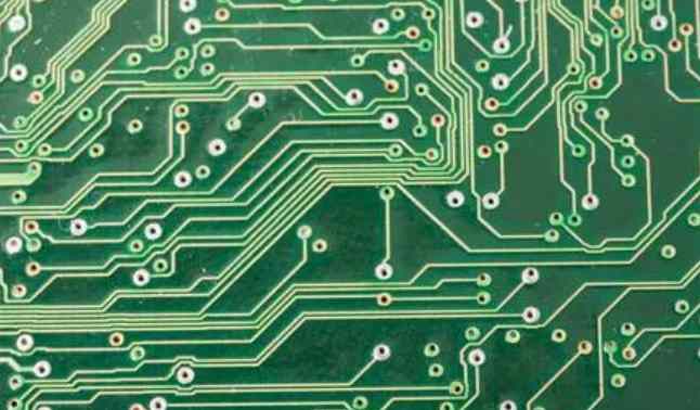
It is very important to control the quality of electroplating copper layer of through-hole printed circuit board. Because the development of multilayer or laminated board to high density, high precision and multi-function direction, the requirements of binding force, uniform fineness, tensile strength and elongation of copper plating layer are more and more strict, and also more and more high, so the quality control of through-hole printed circuit board electroplating is particularly important. Keyou Circuit is committed to PCB proofing and mass production, with high precision single side/double side/multilayer circuit board (1-26 layers), thermoelectric separation copper substrate, multilayer industrial circuit board, power pcb board, medical circuit board, security PCB board, communication PC board, automotive circuit board, instrument circuit board, military circuit board, composite bus copper substrate, Foldable metal substrate, FPC soft and hard combined board, quality assurance, delivery on time, to sales as one of the high-tech enterprises.
First, ensure the uniformity and consistency of the copper plating layer of the through hole printed circuit board. In the process of copper plating of the high aspect ratio printed circuit board, most of them are carried out under the auxiliary action of high-quality additives, with moderate air stirring and cathode movement, under the condition of relatively low current density, so that the electrode reaction control area in the hole is increased, and the role of plating additives can be shown. In addition, the movement of the cathode is very conducive to the improvement of the deep plating ability of the plating solution, the polarization of the plating parts increases, and the formation rate of the crystal nucleus and the growth rate of the grain compensation each other in the electrocrystallization process of the coating, so as to obtain the high toughness copper layer. Of course, the current density is set according to the actual plating area of the printed circuit board being plated. From the analysis of the original understanding of electroplating, the value of current density must also depend on the main salt concentration of high acid and low copper electrolyte, solution temperature, additive content, stirring degree and other factors. In short, the technological parameters and conditions of copper plating must be strictly controlled to ensure that the thickness of the copper plating layer in the hole meets the requirements of the technical standard.
Two, about the use of holes
1. Considering the cost and signal quality, a reasonable hole size is selected. If necessary, consider using different sizes of holes. For example, for power supply or ground wire, consider using larger sizes to reduce impedance, and for signal wiring, use smaller holes. Of course, as the hole size decreases, the corresponding cost will increase.
2. From the two formulas discussed above, it can be concluded that the use of thinner PCB board is beneficial to reduce the two parasitic parameters through the hole.
3. The pins of the power supply and the ground should be drilled into the nearest hole. The shorter the lead between the pins and the hole, the better. Multiple holes may be drilled in parallel to reduce equivalent inductance.
4. Try not to change the layer of signal wiring on PCB board, that is to say, try not to use unnecessary holes.
5. For high density high speed PCB circuit boards, you can consider using micro holes.
6. A number of grounded through-holes are placed near the through-holes of the signal layering to provide the nearest loop for the signal. You can even put some extra ground holes in the PCB board.

Three, about the parasitic inductance through the hole
In the design of high-speed digital circuit, the harm caused by the parasitic inductance is often greater than the influence of the parasitic capacitance. Its parasitic series inductance will weaken the contribution of the bypass capacitance and reduce the filtering effectiveness of the whole power system. The diameter of the hole has little effect on the inductance, while the length of the hole has the biggest effect on the inductance. The impedance generated by the hole can no longer be ignored in the presence of high frequency current. In particular, it should be noted that the bypass capacitor needs to pass through two holes when connecting the power layer to the formation, so that the parasitic inductance of the hole will be multiplied.
The general production process can be divided into cap hole acid etching method and graphic electroplating method, both have advantages and disadvantages. The line obtained by acid etching is very uniform, conducive to impedance control, less environmental pollution, but there is a hole broken will cause scrap; Alkali corrosion production control is easy, but the line is not uniform, the environment pollution is also large.
Precision multilayer circuit board:
1. Precision multilayer PCB circuit board wires are refined and the through-hole is tiny, which improves the requirements on the processing equipment and process control level of PCB circuit board processing plant, and also tests the overall management ability of precision multilayer PCB circuit board factory and the individual ability of employees. 6/6mil line width/line distance fabrication capability, within the current equipment and materials, and process control level, without too much difficulty, can be manufactured by most PCB manufacturers. But from 6/6mil to 5/5mil, is a big leap, many small and medium-sized manufacturers hope to sigh. Seemingly simple, in fact, this requires circuit board manufacturers have strong technical research and development ability and financial strength. Subject to the performance parameters of the exposure machine, etching line processing capacity, and the control ability of the whole process, to achieve 5/5mil line, and maintain a high yield, the overall strength of the plant to support. Similarly, the production of finished aperture 0.3mm and below is also the same (holes below 0.3mm can not be drilled by machine, generally laser drilling) precision multi-layer PCB lines.
2. Other, such as hole without copper, green oil off, gold plate BGA black PAD, weldability, etc., PCB manufacturers commonly encountered problems, should be different people, wisdom. However, PCB board as a special process product, a collection of machinery, electronic control, automation, chemistry, biology, ERP, cost, management, environmental protection and other traditional technology and means, need managers to play great wisdom, need employees to carry forward the spirit, in order to control every detail, maximize the improvement of its quality control ability and level.
3. Guarantee the validity of process detection. As the carrier of all electronic components, PCB reliability is very important. A small hair, a tiny particle of dust, can lead to the entire PCB board scrap, or lead to potential failure. So how is quality guaranteed? It is generally assumed that quality should be manufactured, but it is not. If a PCB factory from the beginning of design, including factory layout, process determination, production equipment selection, manpower allocation, effective evaluation of raw materials, management system determination and other aspects, from the perspective of effective quality control, make corresponding adjustment and control, and prevention of common quality problems, and give full consideration to improve production efficiency, Then the quality control ability and production capacity of this factory in the future will have a good foundation and guarantee. Design work is done well, that is, control the source, lay a good foundation, then the following work is not much easier to do? This is the most effective way to control PCB production process and improve quality.


Just upload Gerber files, BOM files and design files, and the KINGFORD team will provide a complete quotation within 24h.