
Professional PCB manufacturing and assembly
Building 6, Zone 3, Yuekang Road,Bao'an District, Shenzhen, China
+86-13410863085Mon.-Sat.08:00-20:00

Keyou Circuit Technology Co., LTD., is a professional production of high precision double-sided, multi-layer circuit board (1-26 layers), LED aluminum substrate, aluminum circuit board, copper substrate, quality assurance, delivery on time, production and sales as one of the high-tech enterprises.

How much do you know about the structure of aluminum substrate? I believe that most consumers for this problem are not very understanding, because they are not very understanding of aluminum substrate, so in this article, I will be a friend of the circuit will be detailed for you to introduce some structural knowledge about aluminum substrate.
For example, we all know that the main raw material for the production of aluminum substrate is metal plate material, and on its surface is installed a lot of lines, and the main component of aluminum substrate is divided into copper foil material, used for thermal conductivity and insulation layer and metal substrate, and its structure can also be divided into three different layers:
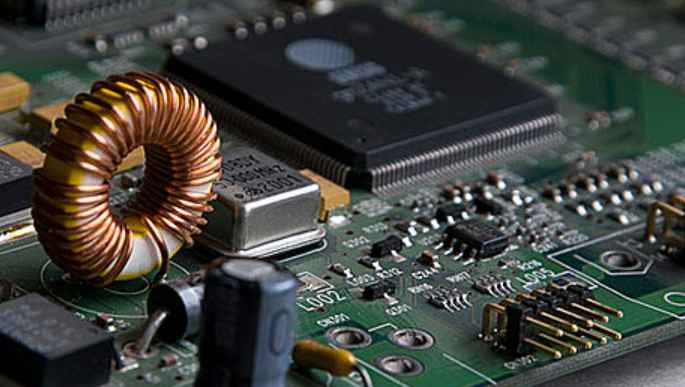
1. It is commonly referred to as the circuit board. Its function is equivalent to the PCB circuit board made of copper materials that we often see, and the circuit board needs to be uniformly covered with a layer of copper foil, but the thickness of copper foil also has a certain range, generally before 1-10oz.
2 is the insulation layer, its main raw materials are insulating materials, so in addition to insulation also has insulation and prevent the role of heat conduction, the thickness of the insulation layer also has a specific range, generally in 0 75 mm to 0 15 mm, and it uses the production technology is the core technology through the national UL technology certification.
3 is the base, that is, we usually say metal substrate, its main raw material is the selection of aluminum material, some manufacturers can also choose brass material as metal substrate production raw materials.
What are the precautions of pcb Mosaic board?
We can discuss together ah, the following first listed 10 need to pay attention to, welcome everyone correct:
1. PCB pieced board should be as close to square as possible. 2×2, 3×3,...... A Mosaic board; But don't spell it as a yin-yang board;
2. The outer frame (clamping edge) of PCB splice board shall adopt closed-loop design to ensure that PCB splice board will not be deformed after fixed on the fixture;
3. The center distance between the small plates is controlled between 75 mm and 145 mm;
4.PCB board width ≤260mm (SIEMENS line) or ≤300mm (FUJI line); If automatic dispensing is required, PCB board width × length ≤125 mm×180 mm;
Keyou Circuit Technology Co., Ltd. was founded in 2003, is committed to PCB proofing and mass production, with high precision single side/double side/multilayer circuit board (1-26 layers), thermoelectric separation copper substrate, multilayer industrial circuit board, power pcb board, medical circuit board, security PCB board, communication PC board, automotive circuit board, Instrument circuit board, military circuit board, composite bus copper substrate, foldable metal substrate, FPC soft and hard combined board, quality assurance, delivery on time, to sales as one of the high-tech enterprises.
5. There should be no large devices or protruding devices near the connection points between the outer frame and the internal small board, small board and small board, and the edge of the components and PCB board should be more than 0.5mm space, to ensure the normal operation of the cutting tool;
6. When setting the reference point, an open weld area 1.5mm larger than the point is usually set aside around the point;
7. Each small board in the PCB assembling board shall have at least three holes, 3≤ aperture ≤6 mm, no wiring or patch is allowed in the edge hole 1mm;
8. Open four holes at the four corners of the outer frame of the plate, with the aperture of 4mm±0.01mm; The strength of the hole should be moderate to ensure that it will not break in the process of upper and lower plate; Aperture and position accuracy should be high, hole wall smooth without burr;
9. Reference symbols for the whole board of PCB and for the fine-spaced devices. In principle, QFP with spacing less than 0.65mm should be set in its diagonal position; Reference symbols for PCB subboards should be used in pairs, arranged diagonally on the elements;
10. Large components should have columns or holes, such as I/O interface, microphone, battery interface, micro switch, headphone interface, motor, etc.;
What are the structural characteristics of aluminum substrate?


Just upload Gerber files, BOM files and design files, and the KINGFORD team will provide a complete quotation within 24h.