
Professional PCB manufacturing and assembly
Building 6, Zone 3, Yuekang Road,Bao'an District, Shenzhen, China
+86-13410863085Mon.-Sat.08:00-20:00

In the world of modern electronic products, PCB (printed circuit board) is an important part of the composition of electronic products, it is hard to imagine in an electronic equipment without PCB, so the quality of PCB will have a great impact on the long-term normal and reliable work of electronic products. Improving the quality of PCB is an important subject that electronic product manufacturers should pay enough attention to.
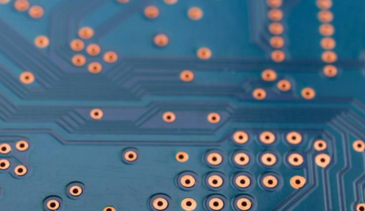
If excessive solder paste is applied on the pad in the PCB assembly process, or insufficient solder paste is added, or even no solder paste is placed, then once the solder joint is formed after the subsequent reflow welding, it will cause defects in the electronic connection between the components and the circuit board. In fact, most defects can be found by virtue of the application of solder paste quality traces.
Currently, many circuit board manufacturers have used some in-circuit tests (ICT), or X-ray techniques, to test the quality of solder joints. They will help eliminate defects arising from the printing process operation, but they cannot monitor the printing process operation itself. A misprinted circuit board may be subjected to additional process steps, each of which increases production costs to varying degrees, leading to a defective circuit board reaching the assembly stage of production. In the end, the manufacturer will have to discard the defective board or accept costly and time-consuming repairs that may not have a clear answer to the root cause of the defect.
Poor solder paste printing process can lead to electronic connection problems. In order to effectively solve this problem, many screen printing equipment manufacturers have adopted online machine vision detection technology, which is briefly introduced below.

Online integrated visual inspection
In order to help circuit board manufacturers in the early stage of production process implementation can find the defects, more and more screen printing equipment manufacturers in their screen printing equipment integrated online machine vision technology. The built-in vision system achieves three main goals:
First, they can detect defects directly after the printing operation, allowing operators to address problems before major manufacturing costs are added to the board. This is usually done when the circuit board is removed from the printing device, after it has been cleaned in the cleaning agent, and after it has been repaired and returned to the production line.
Secondly, because the defects are discovered at this stage, the defective boards can be prevented from reaching the back end of the production line. Thus, the phenomenon of repair or abandonment is prevented in some cases.
Finally, and perhaps most importantly: the ability to give the operator timely feedback on how well the printing process is being operated can effectively prevent defects.
In order to provide effective control during this level of process operation, an on-line vision system is configured to detect the solder pad on the PCB after the solder paste is coated, and whether there is plugging or tailing in the corresponding printing template gaps. In the vast majority of cases, fine-spaced components are tested to optimize testing time and focus on the most problematic areas. For this reason, the time spent in testing is well worth it when the problems that may arise are eliminated.
Specifically, it can be divided into two categories: detection of solder paste on PCB and detection of solder paste on printed template:
a. PCB detection
Mainly detect printing area, printing offset and bridge phenomenon. The detection of the printing area refers to the paste area above each pad. Excessive solder paste may cause the occurrence of bridging phenomenon, and too small solder paste will also cause the phenomenon of unstable welding points. The detection of printing offset is based on whether the amount of solder paste on the pad is different from the specified position. The bridge phenomenon is detected for the application of solder paste between two adjacent pads in excess of the specified amount. The excess paste can cause electrical short circuits.
b. Test the printing template
The detection of printing template is mainly for blocking and tailing. The detection of blockage refers to the detection of the accumulation of solder paste in the holes in the printing template. If the hole is blocked, too little paste may be applied at the next printing point. The detection of tailing refers to whether excessive solder paste has accumulated on the surface of the printed template. This excess paste can be applied to parts of the circuit board that should not be connected, causing electrical connection problems.
Online machine vision systems can benefit PCB manufacturers in different ways. In addition to ensuring a high degree of solder joint integrity, it prevents the manufacturer from wasting money due to defects in the circuit board and the resulting rework. Perhaps most importantly, it provides continuous process feedback, which not only helps manufacturers optimize the screen printing process, but also creates more confidence in the process.

Circuit board temperature is more or less normal
Feb 11,2023


Just upload Gerber files, BOM files and design files, and the KINGFORD team will provide a complete quotation within 24h.