
Professional PCB manufacturing and assembly
Building 6, Zone 3, Yuekang Road,Bao'an District, Shenzhen, China
+86-13410863085Mon.-Sat.08:00-20:00

The digital world is getting more complex every hour, and the hardware associated with it is getting smaller. The advantages of HDI PCBs are many, starting with more interconnects in a smaller area. This leads to miniaturization of circuit boards that can be used for many applications.
The PCB industry plays an important role in the development of all electronic products. Let it be a pacemaker in someone's chest or a motherboard in a programmer's workstation, the PCB makes it possible to manufacture critical electronics.

As component sizes shrink, printed circuit board manufacturers adapt to changing trends. This led to the birth of the HDI design. This enables smaller, denser PCBs with higher component counts and faster speeds.
What is HDI PCB?
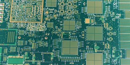
High Density Interconnect (HDI) is simply a PCB with a higher number of interconnects in the smallest footprint. This leads to miniaturization of the circuit board. Components are placed closer together and board space is significantly reduced, but functionality is not compromised.
More precisely, a PCB with an average of 120 to 160 pins per square inch is considered an HDI PCB. HDI designs combine dense component placement and versatile routing. HDI popularized microporous technology. Create denser circuits by implementing microvias, buried vias, and blind vias. Reduced drilling of copper in HDI designs.
What are the advantages of HDI PCB?

Extraordinary Versatility: HDI boards are ideal when weight, space, reliability and performance are the main concerns.
Compact Design: The combination of blind, buried and micro vias reduces board space requirements.
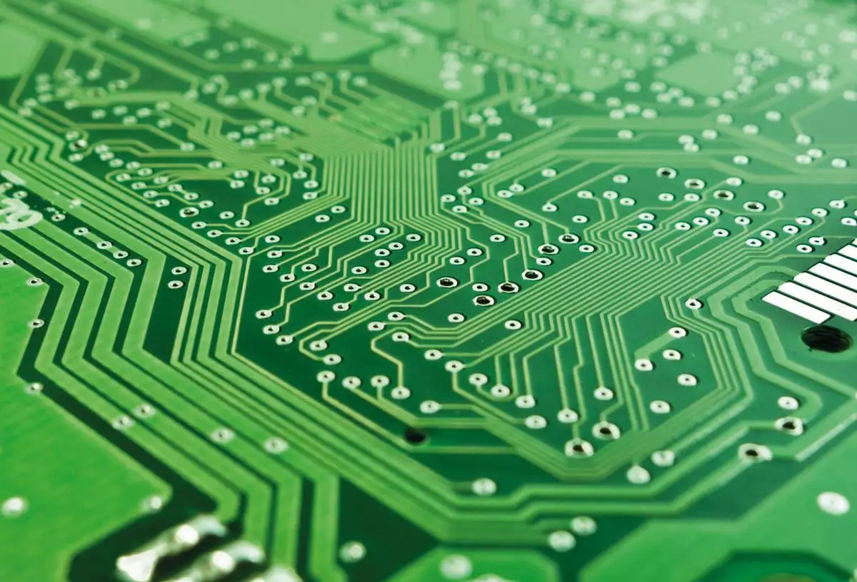
Better Signal Integrity: HDI utilizes via-in-pad and blind via technology. This helps keep components close to each other, reducing signal path lengths. HDI technology removes through-hole stubs, thus reducing signal reflections, thereby improving signal quality. Therefore, it significantly improves signal integrity due to shorter signal paths.
High reliability: The implementation of stacked vias makes these boards a super barrier against extreme environmental conditions.
Cost-effective: The functionality of a standard 8-layer through-hole board (standard PCB) can be reduced to a 6-layer HDI board without compromising quality.
HDI PCB Design Tips
Once you have determined that you need HDI, you need to look at the stack. Do not use more than three consecutive layers unless there is absolutely no other solution. It is recommended that you use a good fan-out strategy for complex ICs, such as BGAs and QFNs - if you plan your fan-out strategy correctly, this will help you reduce the number of consecutive laminations.
The difference between HDI and standard PCB
HDI inherently provides better signal integrity performance than non-HDI because all stray capacitance and inductance are reduced when small blind and buried vias are used. Since there are no stubs, the impedance of the microvia is close to the trace impedance. The stray capacitance of regular vias is much higher, which results in larger impedance discontinuities than microvias. Some notable differences between HDI and traditional PCBs are listed below:
Standard (Through Hole) PCB
Higher component density per square inch Smaller compared to HDI
Smaller, lighter, more functional boards Larger and heavier boards
Implementation of Blind, Buried and Microvias
Laser Direct Drilling Mechanical Drilling
Fewer layers More layers
Compatible with high pin count and low pitch packages May face compatibility issues with low pitch packages
Understanding HDI Stacks and Via Structures
"We spent 10 years at HP designing HDI boards before we realized these were 'more than just small vias'. We've been designing TH multilayers and using small laser-drilled blind vias in BGA breakouts to Instead of larger drilled TH vias. Then we realized that at >600 vias/sec, 20,000 laser drills (or 200,000) cost the same as 200 laser drills. Then, We started looking for ways to replace any mechanical drilling with laser drilling.
We also found space for 2 laser-drilled blind vias between the pads of the BGA, whereas before we only had space for one TH. This leads us to the 'channels' and 'boulevards' created by placing these blind vias on the inner layer. Channels and boulevards are the "recipe" for getting 2X to 4X routing density on inner layers, which means you can reduce the number of signal layers and therefore the number of reference planes.
Go back and look at the HDI boards you've built in the past and measure their "pins per square inch" and "inch per square inch" routing on each layer, and future builds and create a "your own table" to give to people . "
Lamination process and different types of HDI PCB stackup
HDI PCB is a multilayer board composed of dense wiring layers. The boards are held together by a lamination process, and the layers are electrically interconnected using different types of vias.
The lamination process starts with the etching of the inner copper layer. Later, they were separated by partially cured laminates and stacked together like a book, with prepreg layers on top and bottom. The layup is then pressed and heated enough to liquefy the prepreg. These liquefied prepregs cool and stick the layers together.
For blind and buried via stackup, the PCB will go through multiple successive laminations. The higher the number of laminates, the higher the cost of the board.
To increase routing density, designers increase the number of layers, resulting in complex stack-ups. Manufacturers use a sequential lamination process to create such complex designs.
Some common stacking types are mentioned below:
1+N+1 – PCB contains 1 high-density interconnect layer
i+N+i (i≥2) – The PCB contains 2 or more high-density interconnect layers. Microvias on different layers can be staggered or stacked
i+bN+i (i≥2) – including buried vias
Any Layer HDI - All layers of the PCB are high density interconnect layers. This allows free interconnection of conductors on any layer of the PCB with the copper-filled stacked microvia structure
What are the applications of HDI PCB?
Healthcare field
HDI PCBs are having an impact on the medical industry. Medical devices are often HDIs because they can be installed in small devices such as implants, labs, and imaging equipment. Medical devices play a vital role in diagnosing disease and indeed provide life support. For example: pacemakers, diagnostic and monitoring facilities.
With the miniaturized camera size, it is possible to look inside the patient and establish the correct diagnosis. Cameras have gotten smaller, but image quality hasn't suffered. HDI PCB technology makes it possible to accommodate these advancements.
Cameras that need to be inserted through the open end, which some men find frustrating, are reduced in size and have better image clarity. I don't think it will hurt much anymore to have a colonoscopy. Thank God the size of PCBs is decreasing otherwise colonoscopy would keep patients away!
car
Automakers love small PCBs because they save more space inside the car. Integrating electronics to provide a better driving experience has been a major focus for automakers as brands like Tesla roll out futuristic vehicles.
Smartphones and Tablets
All smartphones are HDI PCBs with ELIC (Interconnect per Layer) structure. HDI PCB is responsible for making thinner and smaller portable electronic devices.
Wearable Technology
With the introduction of the Apple Watch and other wearables such as VR headsets, HDI is becoming a major stakeholder in the consumer market. Wearable technology is gaining popularity among the younger crowd due to its superior functionality.
Military and Aerospace
HDI is incorporated into military communications equipment and other strategic equipment such as missiles and defense systems. HDI PCBs are ideal for extreme environments and hazardous conditions, making them ideal for aerospace and military applications.
Design with HDI
“HDI is essential when component spacing requires it or board size requires it. Examples of this include smartphones, wearable technology, and robotics. Properly designed HDI boards can enable smaller boards (board size decrease), or two through-hole (TH) boards can be combined into one board (increased pins per area). Well-designed HDI boards have an average of 2 to 3 times more trace length per layer than thru-hole boards .Some very good HDI designers report 4x performance. So knowing what your current through hole design density performance is, you will be able to determine good HDI design performance. HDI boards are more difficult to plan than traditional multilayer boards, Because multilayer boards only have two degrees of freedom, board size and signal layers.
HDI has a myriad of structures and variables that affect density. To understand how blind vias, skip vias, staggered vias, stacked vias, and buried vias affect density, you have to do a "route test" and use all of these different stackups and structures. By measuring metrics (inch/square inch and pin/square inch), you can create a table that relates these density measurements to the corresponding structures. "
Use HDI PCB design techniques when considering the need to mount on a board of a specific size, or the average number of connections per square inch of the board is very high. If the connection of all parts and test points divided by the size of the board is less than 120 - 130 pins per square inch, then HDI is not required.


Just upload Gerber files, BOM files and design files, and the KINGFORD team will provide a complete quotation within 24h.