
Professional PCB manufacturing and assembly
Building 6, Zone 3, Yuekang Road,Bao'an District, Shenzhen, China
+86-13410863085Mon.-Sat.08:00-20:00

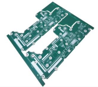
Introduction to the five requirements of HDI production and processing
Circuit board manufacturing, circuit board design and PCBA processing manufacturers explain the five requirements of HDI production and processing
1. HDI Size
[Background Description]
The size of HDI is limited by the capacity of the electronic processing production line equipment, so the appropriate HDI size should be considered in the product system scheme design.
(1) The maximum HDI size that SMT equipment can mount comes from the standard size of HDI sheet, most of which are 20 ″ × 24 ″, i.e. 508mm × 610mm (rail width)
(2) The recommended size is the size of each equipment in the SMT production line, which is conducive to giving play to the production efficiency of each equipment and eliminating equipment bottlenecks.
(3) For small size HDI, it should be designed as a combination to improve the production efficiency of the whole production line.
Design Requirements
(1) In general, the maximum size of HDI shall be limited to 460mm × Within 610mm.
(2) Recommended size range is (200~250) mm × (250~350) mm, and the length width ratio shall be 2.
(3) For size "125mm × The HDI of 125mm shall be assembled into proper size.
2. HDI profile
[Background Description]
The SMT production equipment uses rails to transmit HDI, and cannot transmit HDI with irregular shape, especially HDI with notched corners.
Design Requirements
(1) HDI shape shall be regular square with rounded corners.
(2) In order to ensure the stability of the transmission process, the irregular HDI shall be converted into a standard square by means of plate assembly. In particular, the corner gap should be filled to avoid jamming during the transmission of wave welding gripper.
(3) The pure SMT plate is allowed to have a notch, but the notch size should be less than one third of the length of the side where it is located. For those exceeding this requirement, the design process side should be supplemented.
(4) The chamfering design of golden finger requires chamfering at the insertion side, and the two sides of the insertion plate should also be designed (1~1.5) × 45 ° chamfer to facilitate insertion.
3. Transport side
[Background Description]
The size of the transmission side depends on the requirements of the transmission guide rail of the equipment. For the printing machine, the mounting machine and the reflow welding furnace, the transmission side is generally required to be more than 3.5mm.
Design Requirements
(1) In order to reduce HDI deformation during welding, the long side direction of non assembled HDI is generally taken as the transmission direction; The long side direction shall also be used as the transmission direction for the composition.
(2) Generally, two edges in the HDI or plate assembly transmission direction are used as the transmission edge. The minimum width of the transmission edge is 5.0mm. There shall be no components or solder joints in the front and back sides of the transmission edge.
(3) There are no restrictions on SMT equipment at the non transmission side. It is better to reserve a 2.5mm element forbidden layout area.
4. Locating hole
[Background Description]
Many processes, such as plate assembly, assembly and testing, require HDI accurate positioning. Therefore, it is generally required to design positioning holes.
Design Requirements
(1) Each HDI shall be designed with at least two locating holes, one is designed as a circle, and the other is designed as a long groove. The former is used for locating, and the latter is used for guiding. There is no special requirement for the positioning hole diameter. It can be designed according to the specifications of the factory. The recommended diameters are 2.4mm and 3.0mm. Locating holes shall be non-metallic. If HDI is blanking HDI, the locating hole shall be designed with an orifice plate to enhance the rigidity. The length of the guide hole is generally 2 times of the diameter. The center of the positioning hole should be more than 5.0mm away from the transmission side, and the two positioning holes should be as far away as possible. It is recommended to arrange them at the opposite corners of HDI.
(2) For mixed HDI (HDIA with plug-ins installed), the location of the locating holes should be consistent, so that the front and back of the tooling can be shared. If screws are installed, the bottom bracket can also be used for the tray of plug-ins.
5. Locator
[Background Description]
Modern mounters, printers, optical inspection equipment (AOI), solder paste inspection equipment (SPI), etc. all use optical positioning systems. Therefore, optical location symbols must be designed on HDI.
Design Requirements
(1) Positioning symbols are divided into global positioning symbols (Global Fiducial) and local positioning symbols (Local Fiducial). The former is used for the positioning of the whole board, and the latter is used for the positioning of the assembled sub boards or fine pitch components.
(2) The optical positioning symbol can be designed as a square, diamond shaped circle, cross shaped, well shaped, etc., with a height of 2.0mm. It is generally recommended to design a circular copper definition figure with a diameter of 1.0m. In consideration of the contrast between the material color and the environment, a non blocking welding area 1mm larger than the optical positioning symbol should be reserved. No characters are allowed in it. Whether there is copper foil in the inner layer of the three symbols on the same board should be consistent.
(3) On the HDI surface with SMD components, it is recommended to lay three full board optical positioning symbols at the corners of the board to facilitate the three-dimensional positioning of HDI (three points determine a plane, which can detect the thickness of solder paste).
(4) For the assembly, in addition to three optical positioning symbols for the whole board, it is better to design two or three optical positioning symbols for the assembly at the opposite corners of each unit board.
(5) For QFP with lead wire center distance ≤ 0.5mm and BGA with lead wire center distance ≤ 0.8mm and other devices, local optical positioning symbols shall be set at the opposite corners to facilitate accurate positioning.
(6) If there are mounted components on both sides, each side should have an optical positioning symbol.
(7) If there is no positioning hole on the HDI, the center of the optical positioning symbol shall be more than 6.5 mm from the HDI transmission side. If there is a positioning hole on the HDI, the center of the optical positioning symbol shall be designed at the side where the positioning hole is close to the HDI center. The circuit board manufacturer, circuit board designer and PCBA processor will explain the five requirements for HDI production and processing.


Just upload Gerber files, BOM files and design files, and the KINGFORD team will provide a complete quotation within 24h.