
Professional PCB manufacturing and assembly
Building 6, Zone 3, Yuekang Road,Bao'an District, Shenzhen, China
+86-13410863085Mon.-Sat.08:00-20:00

What are the main materials of FPC packaging substrate?
PCB manufacturers, PCB designers and PCBA manufacturers will explain to you what are the main materials of the packaging substrate for FPCs?
According to FPC manufacturers, packaging substrate is the largest cost of IC packaging, accounting for more than 30%. IC packaging costs include packaging substrate, packaging materials, equipment depreciation and testing, among which the cost of IC carrier plate accounts for more than 30%, which is the major cost of integrated circuit packaging and plays an important role in integrated circuit packaging. For IC carrier plate, its substrate materials include copper foil, substrate, dry film (solid photoresist), wet film (liquid photoresist) and metal materials (copper ball, nickel bead and gold salt). The substrate accounts for more than 30%, which is the largest cost end of IC carrier plate.
1) One of the main raw materials: copper foil
Similar to PCB of FPC factory, the copper foil required for IC carrier plate is also electrolytic copper foil, and it needs to be ultra-thin and uniform copper foil with a minimum thickness of 1.5 μ m. Generally 2-18 μ m. The thickness of copper foil used for traditional PCB is 18 and 35 μ M or so. The price of ultra-thin copper foil is higher than that of ordinary electrolytic copper foil, and it is more difficult to process.
2) The second main raw material: base plate
The base plate of the carrier plate is similar to the copper clad plate of PCB, which is mainly divided into three categories: hard base plate, flexible film base plate and co fired ceramic base plate. The hard base plate and flexible base plate have greater development space, while the development of co fired ceramic base plate tends to slow down.
The main factors to be considered for IC carrier substrate include dimensional stability, high-frequency characteristics, heat resistance, thermal conductivity and other requirements:
At present, there are mainly three kinds of hard packaging substrate materials, namely BT materials, ABF materials and MIS materials;
Flexible packaging substrate substrate materials mainly include PI (polyimide) and PE (polyester) resin;
Ceramic packaging substrate materials are mainly alumina, aluminum nitride, silicon carbide and other ceramic materials.
Hard substrate material: BT, ABF, MIS
1) BT resin The full name of BT resin is "bismaleimide triazine resin", which is developed by Mitsubishi Gas Corporation of Japan. Although the patent period of BT resin has expired, Mitsubishi Gas Corporation is still in the leading position in the world in the research, development and application of BT resin. BT resin has many advantages such as high Tg, high heat resistance, moisture resistance, low dielectric constant (Dk) and low dissipation factor (Df, Therefore, BT materials are mostly used for network chips and programmable logic chips with high reliability requirements. At present, BT substrate is mostly used for mobile phone MEMS chips, communication chips, memory chips and other products. With the rapid development of LED chips, the application of BT substrate in LED chip packaging is also developing rapidly.
2) ABF ABF material is a material led by Intel, which is used to import high-class carrier plates such as Flip Chip. Compared with BT substrate, ABF material can be used as IC with thinner lines and high number of legs and high transmission, and is mostly used for large high-end chips such as CPU, GPU and chipset. As a layer adding material, ABF can be directly attached to the copper foil substrate as a circuit without hot pressing.
In the past, ABFFC had thickness problems. However, due to the increasingly advanced technology of copper foil substrate, ABFFC can solve the thickness problem as long as it uses thin plates. In the early days, most of the ABF carriers were used in the CPU of computers and game consoles. With the rise of smart phones and the change of packaging technology, the ABF industry fell into a low tide. However, in recent years, with the improvement of network speed and technological breakthrough, new applications of high-performance computing have come to the surface, and the demand for ABF has been magnified again.
From the perspective of industry trends, FPC manufacturers believe that ABF substrate can keep up with the pace of advanced semiconductor manufacturing processes, meet the requirements of thin lines, thin line width/line spacing, and have promising market growth potential in the future. Production capacity is limited, and industry leaders begin to expand production.
3) MIS MIS substrate packaging technology is a new technology, which is developing rapidly in analog, power IC, digital currency and other market fields. Different from traditional substrates, MIS includes one or more layers of pre encapsulation structure. Each layer is interconnected by electroplating copper to provide electrical connection in the packaging process. MIS can replace some traditional packages such as QFN package or lead frame based package, because MIS has finer wiring capability, better electrical and thermal performance, and smaller shape.
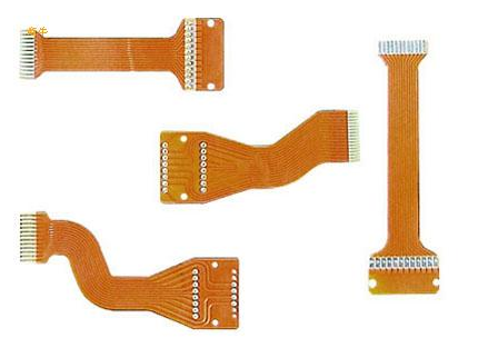
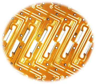
Flexible substrate material: PI, PE
PI and PE resins are widely used in flexible PCB and IC carrier, especially in ribbon IC carrier. The flexible film substrate is mainly divided into three layers of adhesive substrate and two layers of non adhesive substrate. The three-layer rubber plate was originally used for launch vehicles, cruise missiles, space satellites and other military electronic products, and later expanded to various civil electronic product chips; The thickness of rubber free board is smaller, which is suitable for high-density wiring. It has obvious advantages in heat resistance, thin wire and thinness. The products are widely used in consumer electronics, automotive electronics and other fields, and will be the main development direction of flexible packaging substrate in the future. PCB manufacturers, PCB designers and PCBA manufacturers will explain to you what are the main materials of the packaging substrate for FPCs?


Just upload Gerber files, BOM files and design files, and the KINGFORD team will provide a complete quotation within 24h.