
Professional PCB manufacturing and assembly
Building 6, Zone 3, Yuekang Road,Bao'an District, Shenzhen, China
+86-13410863085Mon.-Sat.08:00-20:00

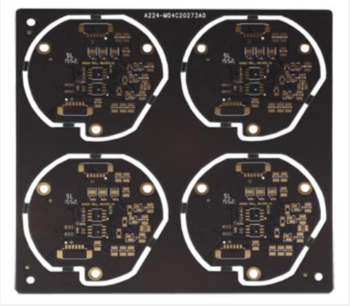
Circuit board manufacturer explains how to solve HDI failure mechanism
Circuit board manufacturer, circuit board design, PCBA processing manufacturer explain to you: circuit board manufacturer explain how to solve HDI failure mechanism
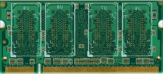
With the development trend of high-precision printed circuit boards, high-density HDI, and the environmental requirements of lead-free and halogen-free, more and more HDIs have various failure problems, such as poor wetting, bursting, delamination, CAF, etc. The application of these analysis techniques in practical cases is introduced. The acquisition of failure mechanism and cause in HDI manufacturing will be conducive to the quality control of HDI in the future, so as to avoid the recurrence of similar problems.
As the carrier of various components and the hub of circuit signal transmission, HDI has become the most important and critical part of electronic information products. Its quality and reliability level determine the quality and reliability of the whole equipment. However, due to the cost and technology, HDI has a lot of failure problems in the production and application process.
It takes a long time to use some commonly used failure analysis techniques. Between the structural characteristics and main failure modes of HDI, this paper will focus on nine technologies used for HDI failure analysis, including: appearance inspection, X-ray fluoroscopy, metallographic section analysis, thermal analysis, photoelectron spectroscopy analysis, micro infrared analysis, scanning electron microscopy analysis and X-ray energy spectroscopy analysis. Among HDI proofing, metallographic section analysis is a destructive analysis technology. Once these two technologies are used, the sample will be damaged and cannot be recovered; In addition, due to the requirements of sample preparation, it may be necessary to partially destroy the sample for scanning electron microscope analysis and X-ray energy dispersive analysis. In addition, in the process of analysis, it may also be necessary to use test technologies such as thermal stress, electrical properties, weldability test and size measurement due to the need of failure location and failure cause verification.
1 Visual inspection Visual inspection is to visually inspect or use some simple instruments, such as stereo microscope, metallographic microscope and even magnifying glass, to check the appearance of HDI, and to find the failure location and relevant physical evidence. Its main function is to locate the failure and preliminarily judge the failure mode of HDI. The appearance inspection mainly checks whether the HDI contamination, corrosion, the location of bursting plates, circuit wiring and the regularity of failure, such as batch or individual, are always concentrated in a certain area, etc. In addition, many HDI failures are discovered after HDIA is assembled. Whether the failure is caused by the influence of the assembly process and the materials used in the process also requires careful inspection of the characteristics of the failure area.
2 X-ray fluoroscopy inspection For some parts that cannot be visually inspected, as well as internal defects of HDI through-hole and other internal defects, X-ray fluoroscopy system must be used for inspection. X-ray fluoroscopy system is to use different principles of moisture absorption or transmissivity of different materials with different thickness or density to image. This technology is more used to check the internal defects of HDIA solder joints, through hole internal defects and the positioning of defective solder joints of high-density BGA or CSP devices. At present, the resolution of industrial X-ray fluoroscopy equipment can reach less than one micrometer, and it is changing from two-dimensional to three-dimensional imaging equipment. Even five dimensional (5D) equipment has been used for packaging inspection, but this 5D X-ray fluoroscopy system is very valuable, and rarely has practical applications in industry.
3 Slice analysis Slice analysis is the process of obtaining HDI cross section structure through a series of means and steps such as sampling, inlaying, slicing, polishing, corrosion and observation. Through slice analysis, we can get rich information of microstructure reflecting HDI manufacturing (through-hole, coating, etc.) quality, which provides a good basis for the next step of quality improvement. However, this method is destructive. Once the sample is sliced, the sample will inevitably be damaged; At the same time, this method requires high sample preparation requirements and takes a long time, which requires well-trained technicians to complete. For detailed slicing operation process, refer to IPC standard IPC-TM-650 2.1.1 and IPC-MS-810.
At present, scanning acoustic microscope is mainly used for electronic packaging or assembly analysis, which is a C-mode ultrasonic scanning acoustic microscope. It uses the amplitude, phase and polarity changes generated by high-frequency ultrasonic reflection on the discontinuous interface of materials to image. Its scanning mode is to scan the X-Y plane information along the Z-axis. Therefore, scanning acoustic microscope can be used to detect various defects in components, materials and HDI and HDIA, including cracks, delaminations, inclusions and cavities. If the frequency width of the scanning acoustic is sufficient, the internal defects of the solder joint can also be directly detected. The typical scanning acoustic image shows the existence of defects in red warning color. Because a large number of plastic encapsulated components are used in the SMT process, during the process of converting from lead to lead-free process, a large number of moisture reflux sensitive problems occur, that is, the hygroscopic plastic encapsulated devices will have internal or substrate delamination cracking when reflowing at higher lead-free process temperature, Under the high temperature of lead-free process, ordinary HDI will often appear plate bursting phenomenon. At this point, the scanning acoustic microscope highlights its special advantages in multi-layer high-density HDI nondestructive testing. Generally, the obvious bursting plate can be detected by visual inspection.
5 Microscopic infrared analysis Microscopic infrared analysis is an analysis method that combines infrared spectrum with microscope. It uses the principle of different absorption of infrared spectrum by different materials (mainly organic substances) to analyze the compound composition of materials, and combines microscope to make visible light and infrared light have the same optical path. As long as you are in the visible field of view, you can find the trace organic pollutants to be analyzed. If there is no combination of microscopes, usually infrared spectroscopy can only analyze samples with a large amount of samples. However, in many cases, micro contamination in electronic processes can lead to poor solderability of HDI factory pads or lead pins. It can be imagined that it is difficult to solve the process problems without the infrared spectrum matching the microscope. The main purpose of micro infrared analysis is to analyze the organic pollutants on the surface of the welded surface or solder joint, and analyze the causes of corrosion or poor weldability. Circuit board manufacturer, circuit board design, PCBA processing manufacturer explain to you: circuit board manufacturer explain how to solve HDI failure mechanism


Just upload Gerber files, BOM files and design files, and the KINGFORD team will provide a complete quotation within 24h.