
Professional PCB manufacturing and assembly
Building 6, Zone 3, Yuekang Road,Bao'an District, Shenzhen, China
+86-13410863085Mon.-Sat.08:00-20:00

How to optimize PCB layer in PCB production must be known.
PCB manufacturers, PCB designers and PCBA manufacturers explain to you how to optimize PCB layers in PCB production.
Layers and their order are also important basic aspects of PCB design. For multilayer SMD packaging, determine the optimal sequence of layers, PCB stacking, and define the construction method of PCB and the function of printed circuit. There are many factors that affect your choice of stacking. The questions that must be answered include how many signal layers are needed, how many ground layers are needed, the thickness of the layers, and what materials should be used. In order to optimize the PCB layer and its layout of the PCB, you need to fully understand the type and characteristics of the PCB layer.
Type of PCB layer
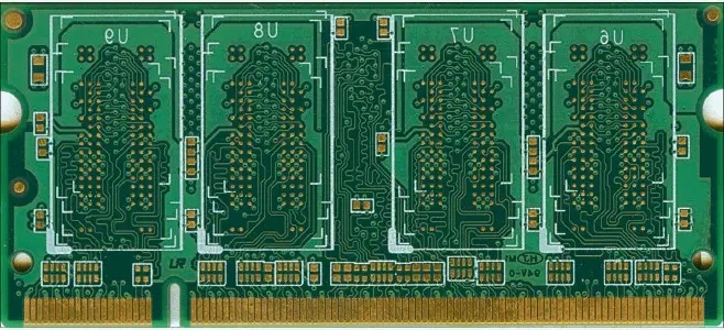
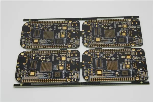
Number of PCB layers PCB structure refers to the number of different layers or layers that will carry signals. The layer type represents the type of signal that will propagate along the layer. Each signal layer or PCB layer is composed of a dielectric material with a copper surface. Most layers are etched. However, the copper surface can also be a solid plane for grounding or energizing. Generally speaking, signal types can be divided into high frequency, low frequency, power supply or grounding. Dielectric and copper may have different design requirements depending on the type of signal.
PCB layer type design requirements
The main materials of PCB layer are dielectric and copper. Dielectric materials provide isolation between different signal types on adjacent layers. This is also the main factor determining the resistivity of PCB. The surface copper of this layer defines the tracking current capacity, resistance and loss. The weight or thickness of copper is used to ensure sufficient current. Closely related to the weight of copper is the tracking width and length, which are used to specify the physical space of each signal path. For high-frequency AC signals, trace matching (length and width) is very important for signal integrity, while for power and ground signals, minimizing losses (corresponding to shorter traces) is very important.
How to optimize PCB layer of PCB
In order to create the best PCB layout for your design, it is necessary to optimize it, which is made and operated by your cm. This can only be achieved through the optimal selection of the stack and the PCB layers it consists of. Following these tips will help you achieve these goals.
PCB layer stacking skills
Tip 1: Determine your motherboard signal type
The type of signal that appears on the board and on the board is the most important factor in selecting stacks and layers. For special and multi signal processing, you are likely to need more layers due to isolation and different reasons.
Tip 2: Determine the number and type of vias
Another factor that determines stacking requirements is through choice. For example, if you choose to bury vias, additional internal layers may be required.
Tip 3: Determine the number of signal layers required
After determining the signal type and vias, you can design the stack by defining the required number of layers and their types.
Tip 4: Determine the number of aircraft required
Select your power and ground planes so they can be used to shield the signal layer and reduce EMI.
Tips for selecting PCB layers
Tip 1: Define the layer according to the signal type
In order to determine the best parameters or material properties, each layer needs to be classified according to its function or the type of signal it will carry.
Prompt 2: Select layer dielectric and copper according to signal requirements
After classifying the layers, you can select their dielectric constant and copper value. These choices will seriously affect the mechanical, electrical, thermal and chemical properties of each layer. However, other material attributes should also be considered to optimize your selection based on their importance to the PCB layer type.
Only by following good examples to make the best material selection and working with the CM that can achieve your selection can the PCB layer of the PCB be optimized. PCB manufacturers, PCB designers and PCBA manufacturers explain how to optimize PCB layers in PCB production.


Just upload Gerber files, BOM files and design files, and the KINGFORD team will provide a complete quotation within 24h.