
Professional PCB manufacturing and assembly
Building 6, Zone 3, Yuekang Road,Bao'an District, Shenzhen, China
+86-13410863085Mon.-Sat.08:00-20:00

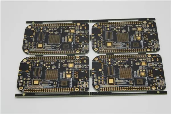
Pcb design plus test points and differentiation of nickel palladium and nickel gold electroplating
PCB manufacturers, PCB designers and PCBA processors will explain how to differentiate nickel palladium gold from electroplated nickel gold by adding test points to PCB design.
Many newcomers often confuse nickel palladium plating with nickel gold plating. What is the difference between nickel palladium plating and nickel gold plating on automobile circuit boards?
Nickel palladium plating is a non selective surface processing technology that uses chemical methods to deposit a layer of nickel, palladium and gold on the surface of the copper layer of the printed circuit board during the proofing of the automobile circuit board.
Electroplating nickel gold refers to making gold particles attach to automobile circuit board by electroplating. It is also called hard gold because of its strong adhesion; The process can greatly increase the hardness and wear resistance of automobile circuit board, and can effectively prevent the diffusion of copper and other metals.
Differences between chemical nickel palladium gold and electroplated nickel gold
Similarities:
1. All belong to the important surface treatment process in automobile circuit board proofing;
2. The main application field is the wiring connection process, which should be applied to medium and high-end electronic circuit products.
difference:
Disadvantages:
1. The common chemical reaction process is adopted for nickel palladium, and the chemical reaction rate is low;
2. The liquid medicine system of nickel palladium is more complex and requires higher production management and quality management.
advantage:
1. Nickel palladium alloy adopts lead-free gold plating process, which can better deal with more precise and high-end electronic circuits;
2. The comprehensive production cost of nickel palladium is lower;
3. Ni-Pd has no tip discharge effect and has higher advantages in controlling the arc ratio of gold finger;
4. Nickel palladium alloy has great advantages in comprehensive production capacity because it does not need lead wire and electroplating wire connection.
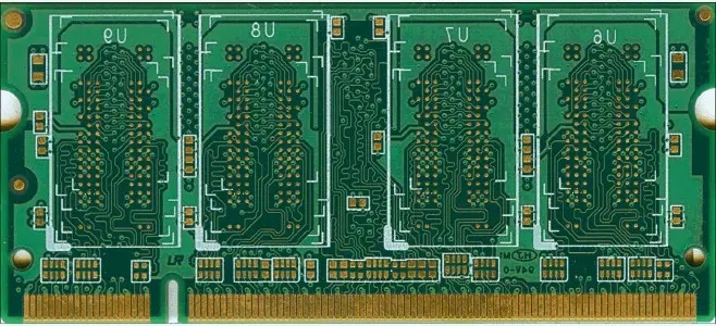
Why should I add test points for 5G PCB design?
The 5G circuit board design and test points are not required for the production of 5G circuit boards, but for ICT testing after the completion of 5G circuit board A, to test whether the 5G circuit board has problems in welding and whether the performance meets the requirements.
During the production of 5G circuit boards, 5G circuit boards also need to be tested to see if there is any open circuit or short circuit. This is useful for testing the needle bed against each network point.
The light board 5G circuit board is OK, but the 5G circuit board is not the same when it is pasted. The components are all welded. Especially for SMT components, what should we do if we use a needle bed and it is easy to damage SMT components when the needle is punctured? It is necessary to add additional test points on each line network for connection of the needle bed. In this way, the needle bed will not damage the SMT components, and the needle bed will press to the flat test point. The test will be more accurate. In the early years, it was stipulated that 90% of the networks should have test points.
There are some unavoidable shortcomings in using a needle bed for testing. There is a limit to the size of the needle and the minimum distance between needles. It may be difficult for high-density PCB.
There are still so many test points. For high-density PCB space, it is really hard to reach. It must be unrealistic. There are a lot of test points now, and there are other test methods. For example, JTAG test, X-REY test, AOI test. However, in some places, these tests cannot replace ICT tests 100%. PCB manufacturers, PCB designers and PCBA processors will explain how to differentiate nickel palladium gold from electroplated nickel gold by adding test points to PCB design.


Just upload Gerber files, BOM files and design files, and the KINGFORD team will provide a complete quotation within 24h.