
Professional PCB manufacturing and assembly
Building 6, Zone 3, Yuekang Road,Bao'an District, Shenzhen, China
+86-13410863085Mon.-Sat.08:00-20:00

We often see in textbooks or IC manufacturers' guides that at the end of, we should coat the outer layer of PCB with copper, that is, use well grounded copper foil to cover the blank area.
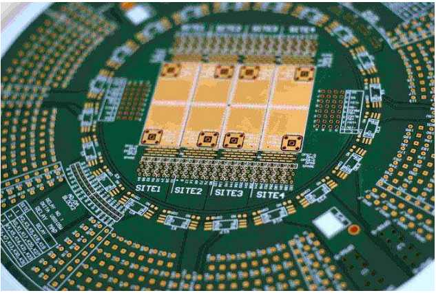
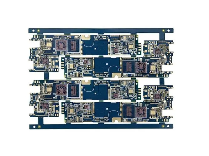
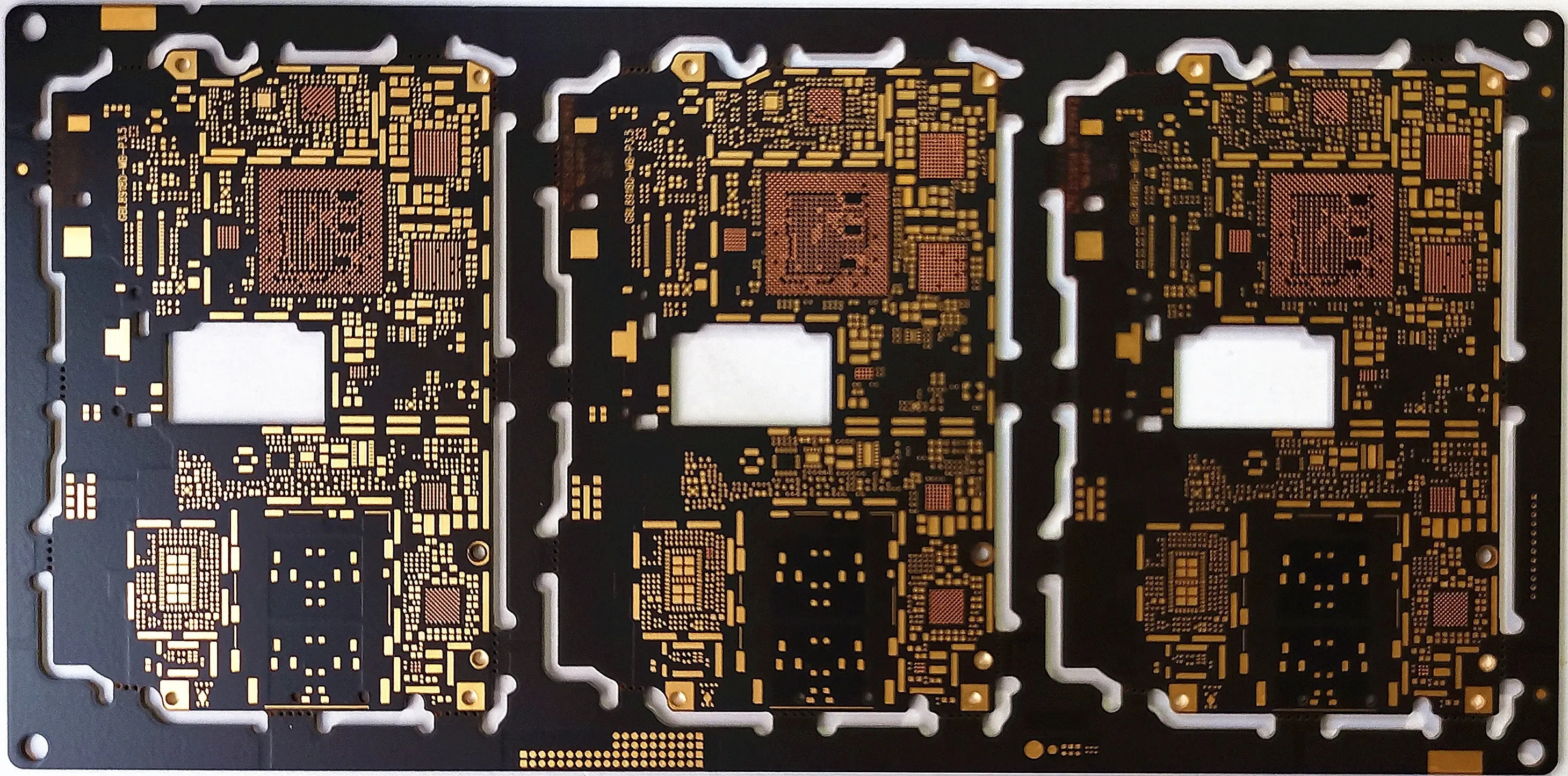
Pcb design
The advantages of copper coating on the outer layer of PCB are as follows:
Provide additional shielding protection and noise suppression for the inner signal to improve the heat dissipation capacity of PCB. During PCB production, save the amount of etchant. (Can this reduce the cost?) Avoid PCB warping and deformation due to different stress caused by over reflow soldering of PCB due to uneven copper foil
But doing so also brings some disadvantages:
The copper clad surface of the outer layer must be separated and fragmented by the surface components and signal wires. If there is a copper foil with poor grounding (especially the thin and long copper scrap), it will become an antenna, resulting in EMI problems. If the copper clad pins are fully connected, it will cause too fast heat loss, resulting in difficulties in disassembly and repair welding. As mentioned earlier, the copper clad surface of the outer layer must be well grounded, It is necessary to drill more vias to connect with the main ground plane. If there are too many vias, the wiring channel will be affected, unless buried blind holes are used.
Pcb design is very necessary for two-layer boards. generally, the ground plane is paved on the bottom layer, and the main devices and power and signal lines are placed on the top layer. For high impedance circuits, analog circuits (analog to digital conversion circuits, switching mode power conversion circuits), copper coating is a good practice.
For multilayer board high-speed digital circuits with complete power supply and ground plane, please note that this refers to high-speed digital circuits. Copper coating on the outer layer will not bring great benefits. For digital circuits with multilayer boards, the inner layer has a complete power supply and ground plane, and copper coating on the surface layer cannot significantly reduce crosstalk. On the contrary, too close to the copper sheet will change the impedance of microstrip transmission lines, and discontinuous copper sheets will also cause a negative impact on the impedance of transmission lines.
For multilayer boards, if the distance between the microstrip line and the reference plane is less than 10mil, the return path of the signal will directly choose the reference plane below the signal line instead of the surrounding copper sheet, because its impedance is lower. For the double-layer plate with a distance of 60 mil between the signal line and the reference plane, the noise can be significantly reduced by wrapping a complete copper sheet along the whole signal line path.
Therefore, whether to lay copper on the surface depends on the application scenario. In addition to the need to wrap the ground for sensitive signals, if there are many high-speed signal lines and components, many small and long copper scrap will be generated, and the wiring channel is tight, it is necessary to avoid the copper skin on the surface from punching holes to connect with the ground plane. At this time, the surface can choose not to lay copper. If there are few PCB components and high-speed signals on the surface layer and the board is relatively open, copper can be paved on the surface layer to meet the requirements of PCB processing technology, but it should be noted that the distance between the copper sheet and high-speed signal line should be at least 4W during pcb design to avoid changing the characteristic impedance of the signal line, and the copper sheet on the surface layer should be well connected with the main ground plane by drilling holes at a wavelength interval of 10% of the highest signal frequency.


Just upload Gerber files, BOM files and design files, and the KINGFORD team will provide a complete quotation within 24h.