
Professional PCB manufacturing and assembly
Building 6, Zone 3, Yuekang Road,Bao'an District, Shenzhen, China
+86-13410863085Mon.-Sat.08:00-20:00

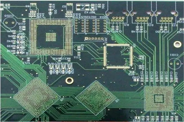
Precision coincidence between poor tin on PCB and multilayer blind buried PCB
PCB manufacturers, PCB designers and PCBA manufacturers explain the precision coincidence between poor tin on PCB and multi-layer blind buried PCB
When SMT is used to produce the SMT, the PCB will not have good tin coating. Generally, the poor tin coating is related to the cleanliness of the bare PCB surface. If there is no dirt, there will be basically no poor tin coating. Secondly, the soldering flux itself is poor when tin coating, temperature, etc. So what are the main manifestations of common electrolytic tin defects in PCB production and processing? How to solve this problem?
1. The tin surface of the base plate or parts is seriously oxidized and the copper surface is dark.
2. The circuit board surface has flake tin, and the coating on the board surface has particle impurities.
3. The high potential coating is rough, there is burning phenomenon, and the plate surface has a sheet shape that cannot be electrified with tin.
4. The circuit board surface is attached with grease, impurities and other sundries, or there is silicone oil residue.
5. There is obvious bright edge at the edge of low potential hole, and the high potential coating is rough, and there is plate burning.
6. The coating on one side is complete, the coating on the other side is poor, and there is obvious bright edge at the edge of low potential hole.
7. The PCB board is not guaranteed to meet the temperature or time during welding, or the flux is not used correctly.
8. The coating on the circuit board surface has particle impurities, or there are grinding particles left on the circuit surface during the production of the substrate.
9. The low potential large area can not be coated with tin, the circuit board surface has fine dark red or red, one side has complete coating, and the other side has poor coating.
Improvement and prevention plan for the bad condition of electrolytic tin on PCB:
1. Strengthen pretreatment before plating.
2. Use flux correctly.
3. Hatch groove analysis and adjustment of polish content.
4. Check the consumption of anode irregularly and add anode reasonably.
5. Reduce the current density, maintain the filtering system regularly or conduct weak electrolysis treatment.
6. Strictly control the storage time and environmental conditions during the storage process, and strictly operate the circuit board manufacturing process.
7. Control the temperature of PCB during welding at 55-80 ℃ and ensure that there is sufficient preheating time.
8. The liquid medicine composition shall be tested and analyzed regularly and added in time, the current density shall be added, and the electroplating time shall be extended.
9. Use solvent to clean sundries. If it is silicone oil, special cleaning solvent shall be used for cleaning.
10. Reasonably adjust the anode distribution, reduce the current density appropriately, reasonably plan the wiring or splicing of boards, and adjust the polish.
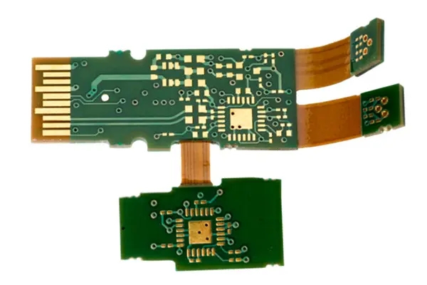
Precise Coincidence of Multilayer Blind Buried PCB
The printed circuit board with multilayer blind buried and blind hole structure is generally completed by the "separate board" production method, which means that it can only be completed after multiple platens, drilling, hole plating, etc., so precise positioning is very important.
High precision of printed circuit refers to the adoption of technologies such as fine line width/spacing, micro holes, narrow ring width (or no ring width), buried and blind holes to achieve high density. High precision means that the result of "thin, small, narrow and thin" will inevitably lead to the requirement of high precision. Take the line width as an example: O.20mm line width is qualified if O.16-0.24mm is produced as required, and the error is (O.20 ± 0.04) mm; Similarly, the error of O.10mm linewidth is (0.10 ± O.02) mm. Obviously, the accuracy of the latter is doubled. It is easy to understand the analogy. Therefore, the requirements for high accuracy will not be discussed separately.
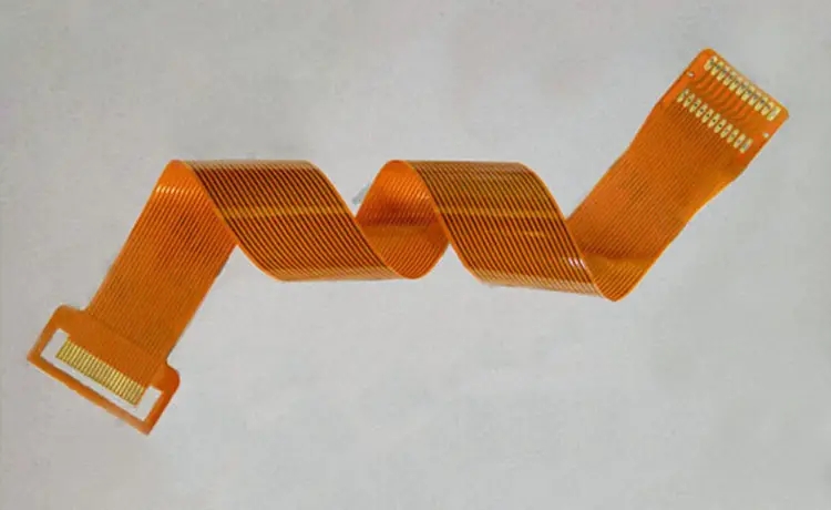
The combination technology of buried, blind and through hole (multilayer blind buried PCB) is also an important way to improve the high-density of printed circuit. Generally, the buried and blind holes are micro holes. In addition to increasing the number of wiring on the circuit board, the buried and blind holes use the "nearest" inter layer interconnection, which greatly reduces the number of vias formed and the setting of isolation panels, thus increasing the number of effective wiring and inter layer interconnection in the board and improving the high-density interconnection.
Interlayer Coincidence in Fabrication of Blind Buried Hole Multilayer Circuit Boards
By using the pin front positioning system produced by ordinary multilayer circuit boards, the graphic production of each layer of a single chip is unified into a positioning system, which creates conditions for the success of manufacturing. For the ultra thick single piece like this one, if the plate thickness reaches 2mm, a certain thickness layer can be milled at the location of the positioning hole, which is also included in the processing capacity of the four slot positioning hole punching equipment of the front positioning system.
PCB manufacturers, PCB designers, and PCBA processors will explain the precision coincidence between poor tin on PCB and multi-layer blind buried PCB.


Just upload Gerber files, BOM files and design files, and the KINGFORD team will provide a complete quotation within 24h.