
Professional PCB manufacturing and assembly
Building 6, Zone 3, Yuekang Road,Bao'an District, Shenzhen, China
+86-13410863085Mon.-Sat.08:00-20:00

Reasons for the high cost of multi-layer PCB proofing and tin plate/gold plate
PCB manufacturing, PCB design and PCBA processing manufacturers explain the reason why multi-layer PCB proofing is expensive and the production process of PCB double-sided circuit board tinplate/gilt plate
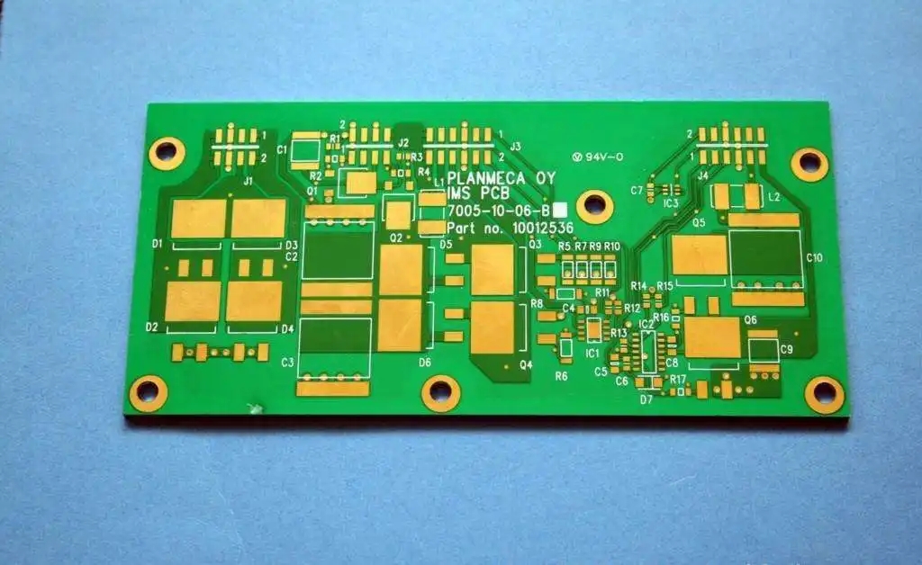
Multilayer PCB is the "core main force" in communication, medical treatment, industrial control, security, automobile, power, aviation, military industry, computer peripheral and other fields. The product function is getting higher and higher, the PCB is getting more and more precise, and the production difficulty is getting more and more difficult. The higher the corresponding number of layers, the higher the cost of PCB proofing of multilayer circuit board. So what are the difficulties in multi-layer PCB manufacturing? Next, let's introduce Shenzhen PCBA manufacturer.
1. Difficulties in making inner circuit of multi-layer PCB proofing
Multilayer board circuit has various special requirements for high speed, thick copper, high frequency and high Tg value, and the requirements for inner layer wiring and graphic size control are getting higher and higher. For example, there are many impedance signal lines in the inner layer of the ARM development board. To ensure the integrity of the impedance increases the difficulty of the inner layer circuit production.
There are many signal lines in the inner layer, and the width and spacing of lines are basically about 4mil or less; The thin production of multi core board is easy to wrinkle, and these factors will increase the production cost of the inner layer.
Suggestion: The line width and line spacing shall be designed to be more than 3.5/3.5mil (most factories have no difficulty in production).
For example, six layer board, it is recommended to use a pseudo eight layer structure design, which can meet the impedance requirements of 50 ohm, 90 ohm and 100 ohm line widths of 4-6 mil inner layers.
2. Difficulties in alignment between inner layers of multi-layer PCB proofing
The number of layers of multilayer board is increasing, and the alignment requirements of the inner layer are also getting higher and higher. Film will expand and shrink due to the influence of workshop environment temperature and humidity, and the core board will expand and shrink the same after production, which makes the alignment accuracy between inner layers more difficult to control.
3. Difficulties in multi-layer PCB proofing and pressing process
The superposition of multiple core plates and PP (prepreg) is prone to delamination, slide plate and steam drum residue during pressing. In the structural design process of the inner layer, we should consider the dielectric thickness between layers, glue flow, heat resistance of the plate and other factors to reasonably design the corresponding laminated structure.
Suggestion: Keep the inner layer of copper evenly paved, and the balance of copper paved in different areas of large area is the same as that of PAD.
4. Difficulties in multi-layer PCB proofing and drilling production
Multilayer boards adopt high Tg or other special boards. The roughness of drilling holes made of different materials is different, which increases the difficulty of removing the glue residue in the holes. The high-density multilayer board has high hole density, low production efficiency and is easy to break the tool. The hole edge between holes of different networks is too close, which will lead to the CAF effect problem. Suggestion: the distance between hole edges of different networks shall be ≥ 0.3mm.
Manufacturing process of PCB double-sided circuit board tin plate/gold plate
Manufacturing process of PCB double-sided circuit board tin plate/gold plate:
Cutting ------ drilling ------ copper sinking ------ circuit ------ electric drawing ------ etching ------ solder resistance ------ characters ------ tin spraying (or gold sinking) - gong edge - v cutting (some boards do not need) ------ flying pin test ------ vacuum packaging
Manufacturing process of gold plated PCB double-sided circuit board:
Cutting ------ drilling ------ copper sinking ------ circuit ------ electric drawing ------ gold plating ------ etching ------ solder resistance ------ characters ------ gong edge ------ v-cutting ------ flying pin test ------ vacuum packaging
Manufacturing process of multi-layer circuit board tin plate/gold plate:
Cutting ------ inner layer ------ laminating ------ drilling ------ copper sinking ------ circuit ------ diagram electricity ------ etching ------ solder resistance ------ characters ------ tin spraying (or gold sinking) ------ gong edge ------ v cutting (some boards do not need) ------ flying test ------ vacuum packaging
Manufacturing process of multilayer circuit board gold-plated board:
Cutting ------ inner layer ------ laminating ------ drilling ------ copper sinking ------ circuit ------ electric drawing ------ gold plating ------ etching ------ solder resistance ------ characters ------ gong edge ------ v cutting ------ flying test ------ vacuum packaging
PCB manufacturing, PCB design and PCBA processing manufacturers will explain to you the reason why multi-layer PCB proofing is expensive and the production process of PCB double-sided circuit board tin plate/gilt plate.


Just upload Gerber files, BOM files and design files, and the KINGFORD team will provide a complete quotation within 24h.