
Professional PCB manufacturing and assembly
Building 6, Zone 3, Yuekang Road,Bao'an District, Shenzhen, China
+86-13410863085Mon.-Sat.08:00-20:00

Printed circuit mark and identification method of PCB and gold finger of circuit board
PCB manufacturers, PCB designers and PCBA manufacturers will explain PCB printed circuit signs and identification methods and PCB gold fingers
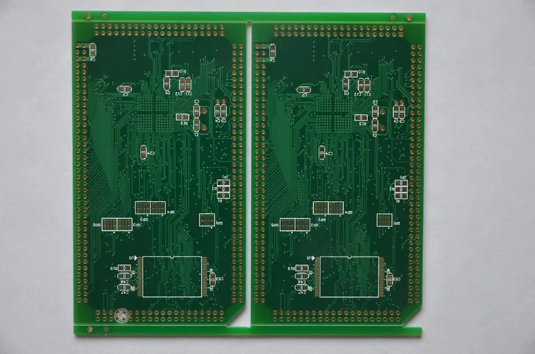
Almost all printed circuits are required to be printed on the PCB with names to identify components, circuits, test points and the PCB itself. The circuit board factory also attaches great importance to this aspect. With curiosity, we went to the circuit board factory to learn about the small knowledge related to printed circuit signs and identification.
In PCB fabrication, the name can be printed after the PCB is etched, or etched at the same time as the circuit is etched. If it is printed in the future, it is usually printed with a screen leak printing process, or stamped with a seal. In either case, in order to ensure the electrical and chemical characteristics, the marking materials must be carefully selected. Considering this principle and some additional process steps involved, usually the designer should have a name on its photographic base and etch the circuit at the same time. Although these names are conductive, they generally do not cause problems. The handwriting of the names should be small enough to withstand etching and be clearly visible. The thickness of the copper foil and the position of the name relative to the wire will determine how much the name will be damaged during etching. When using 2 ounces of 3 ounces of copper foil, the name is too small to see clearly.
In order to facilitate the testing and maintenance of a printed board assembly, and to facilitate the visual inspection of the assembly against the drawing data, the reference name mark of the component should be considered. In addition to the reference name mark, the polarity of capacitor and diode should be pointed out and marked as close as possible to its mounting hole. The reference name and polarity should be completely visible at the place where the element is placed. The No. 1 lead of the dual in-line integrated circuit should always be marked, and the TO-5 integrated circuit with No. 6, 8, 10 or 12 lead should also be marked.
The printed circuit board should have two identification marks of different properties, because before the assembly of electrical components, the manufacturer needs to machine and coat the printed circuit board, and it needs to use documents and a method to identify the printed circuit board. One is the manufacturing drawing number (original drawing number) of the printed circuit board, and the other is the number of the assembly parts of the printed circuit board should also be marked on one side of the component. Electrical components should be assembled on this side of the component, and spare components should be replaced. Usually, testing and maintenance are also carried out here. The numbering should always be continued according to "ASSYNO". In addition, for searching, printed board assemblies must be numbered consecutively. If space allows, your company name can be displayed on the printed board. All these requirements can be easily made by etching foil.
PCB circuit board gold finger
The so-called circuit board gold finger refers to a row of square bonding pads arranged at equal intervals, exposed copper and plated with gold. It is mainly used for electrical connection pins connecting boards, LCD, mainboards, chassis, etc., because a thin layer of gold is plated on the copper foil nickel coating.
1、 Definition and function of PCB gold finger:
GoldFinger: (GoldFinger or EdgeConnector) insert one end of the PCB into the connector slot, use the connector pin as the outlet of the external connection of the PCB, make the pad or copper sheet contact with the pin at the corresponding position to achieve the purpose of continuity, and coat the pad or copper sheet of the PCB with nickel gold, It is called golden finger because of its shape. Gold was chosen because of its superior conductivity, oxidation resistance and wear resistance. However, because of its high cost, gold is only used for local gold plating such as golden finger.
2、 Classification and recognition characteristics of circuit board gold finger
Golden finger classification of circuit boards:
1. Regular golden finger (flush finger);
2. Segmented golden finger (intermittent golden finger);
3. Long and short golden fingers (that is, uneven golden fingers).
Gold finger circuit board with different lengths
Regular gold fingers (flush fingers): rectangular pads of the same length and width are arranged at the edge of the board. The following figure shows that there are many gold fingers for objects such as network cards and video cards, while there are few gold fingers for some small boards;
2. Segmented gold finger (discontinuous gold finger): rectangular pads with different lengths at the edge of the plate, and the front section is disconnected;
3. Long and short gold fingers (i.e. uneven gold fingers): rectangular pads with different lengths at the edge of the plate.
Features: There is no character frame and mark, and it is generally a window for the solder mask. Most of the shapes have grooves. The gold finger part protrudes from the board edge or is close to the board edge. Some boards have gold fingers at both ends. Normal gold fingers are on both sides. Some PCB circuit boards have only one side of the gold finger. Some circuit boards have a wide single gold finger.
PCB manufacturers, PCB designers and PCBA manufacturers will explain PCB printed circuit signs and identification methods, as well as PCB gold fingers.


Just upload Gerber files, BOM files and design files, and the KINGFORD team will provide a complete quotation within 24h.