
Professional PCB manufacturing and assembly
Building 6, Zone 3, Yuekang Road,Bao'an District, Shenzhen, China
+86-13410863085Mon.-Sat.08:00-20:00

The problem of component displacement during SMT chip processing is actually a bad phenomenon in SMT factory processing. With the development of science and technology and the improvement of people's living standards, the pursuit of electronic products is becoming increasingly miniaturized and sophisticated. However, the traditional DIP plug-ins in SMT small batch SMT chip processing plants play a less important role in small compact PCBA than SMT chip processing, especially in large-scale, highly integrated ICs. For many R&D companies, it is a good choice to send products to SMT small batch patch processing plants to adopt the PCBA processing method of SMT labor and materials contracting. However, there are also some problems in SMT chip processing, such as component displacement. What is the matter of SMT chip processing component displacement.
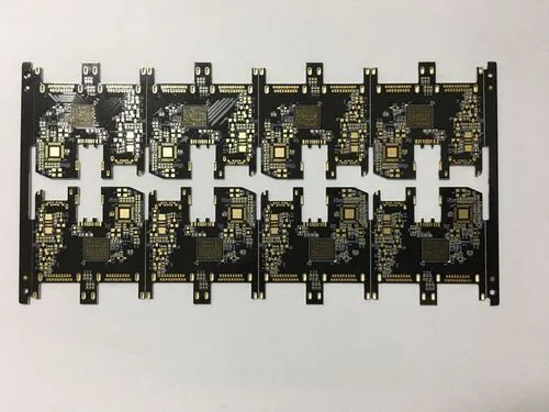
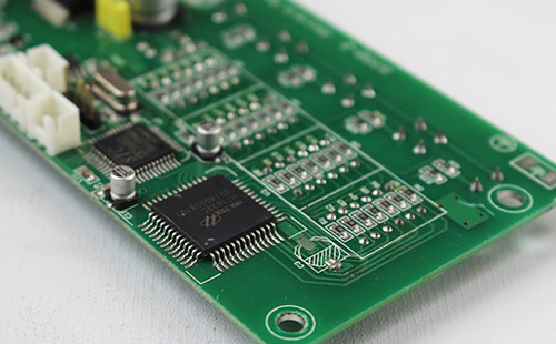
SMT chip processing
1、 When the air pressure of the suction nozzle is not adjusted properly, the pressure is not enough to cause the displacement of components.
2、 The flux content in the solder paste is too high, and excessive flux flow during reflow leads to component displacement.
3、 The solder paste itself is not sticky enough, and the components vibrate and shake during handling, which causes the components to shift.
4、 The use time of solder paste is limited. After the service life of SMT solder paste is exceeded, the flux in it deteriorates, resulting in poor welding of PCBA patch.
5、 During the handling of components after SMT printing and PCBA mounting, the components are displaced due to vibration or incorrect handling methods.
6、 The placement position of components is incorrect due to the mechanical problems of the mounter itself. Every step of SMT labor and material contracting should be done carefully, and the PCBA processing process should be strictly followed. Good service attitude can bring high-quality PCBA products.
Differences between lead-free and lead-free processes in SMT chip processing
Generally, there are two processes, one is lead-free process and the other is leaded process. Everyone knows that lead is harmful to people. Therefore, lead-free process meets the requirements of environmental protection and is the trend of the times. Shenzhen Yingchuang Electronic SMT chip OEM materials are all lead-free process.
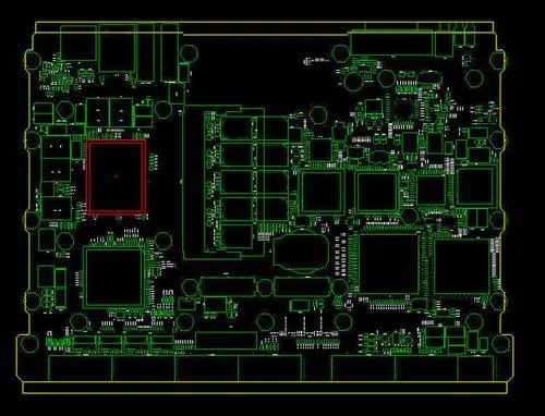
SMT chip processing
The difference between leaded process and lead-free process is briefly summarized as follows:
1. The alloy composition is different: the common lead process tin lead composition is 63/37, while the lead-free alloy composition is SAC305, that is, Sn: 96.5%, Ag: 3%, Cu: 0.5%. Lead free process cannot absolutely guarantee that there is no lead at all, only lead with very low content, such as lead below 500PPM.
2. Different melting points: the melting point of lead tin is 180 °~185 °, and the working temperature is about 240 °~250 °. The melting point of lead-free tin is 210 °~235 °, and the working temperature is 245 °~280 °. According to experience, for every 8% - 10% increase in tin content, the melting point will increase by about 10 ℃, and the working temperature will increase by 10-20 ℃.
3. The cost is different: the price of tin is more expensive than that of lead. When lead is replaced with tin by solder of equal importance, the cost of solder will rise significantly. Therefore, the cost of lead-free process is much higher than that of lead process. Statistics show that the cost of lead-free process is 2.7 times higher than that of lead process for wave soldering and manual soldering, and the cost of solder paste for reflow soldering is about 1.5 times higher.
4. Different processes: lead process and lead-free process can be seen from the name. However, when it comes to PCB process, the solder, PCB components and equipment used are different, such as wave soldering furnace, solder paste printer, and soldering iron used for manual soldering.
Other differences, such as process window, weldability, environmental requirements, are also different. The lead process has a larger process window, better solderability, and the lead-free process is more in line with environmental requirements. With the continuous progress of technology, the lead-free process technology has become increasingly reliable and mature.


Just upload Gerber files, BOM files and design files, and the KINGFORD team will provide a complete quotation within 24h.