
Professional PCB manufacturing and assembly
Building 6, Zone 3, Yuekang Road,Bao'an District, Shenzhen, China
+86-13410863085Mon.-Sat.08:00-20:00

Brief Introduction of the Key Process of Double sided Printed Board Manufacturing
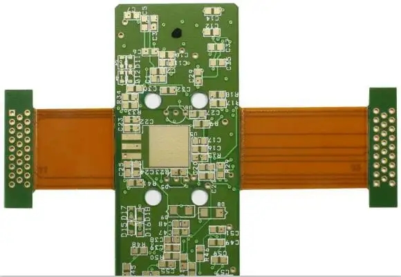
Double sided PCB refers to the printed board with conductive graphics on both sides. It is usually made of epoxy glass cloth copper clad foil, and is mainly used in communication electronic equipment, advanced instruments and meters, electronic computers and other equipment with high performance requirements.
1. CNC drilling
Due to the development of SMT (Surface Mount Technology), the plated holes on the printed board are no longer used for inserting electronic components, but only used for guiding. In order to improve the assembly density, the holes become smaller and smaller, so a new generation of CNC drilling machine that can drill tiny holes is often used for processing. The drilling speed of this NC drilling machine is 110 000 ~ 150 000 r/min, and it can drill holes with diameters of 0.1 ~ 0.5 mm. If the drill bit is broken, it will automatically stop and alarm, automatically replace the drill bit and measure the drill bit diameter, automatically control the constant distance and drilling depth between the drill bit and the cover plate, so that it can not only drill through holes, but also drill blind holes.
2. Hole plating process
Plated hole (PTH) is also known as metallized hole. The whole hole wall is plated with metal, so that the conductive patterns between the two sides of the double-sided printed board or the inner and outer layers of the multilayer printed board can be electrically connected. Metallized hole is the most critical link in the production process of double-sided board and multilayer board, which is related to the internal quality of multilayer board. Traditionally, electroless copper plating is used to deposit a thin layer of copper on the hole wall, and then the electroplating copper is thickened to the specified thickness. Some new hole plating processes have been developed, such as direct electroplating without electroless copper plating.
3. Imaging
Screen printing imaging can also be used to make double-sided plates. It is low cost and suitable for mass production, but it is difficult to make fine wires below 0.2mm and double-sided plates with fine spacing. In addition to screen printing, polyvinyl alcohol/dichromate type liquid photoresist was widely used in the 1950s and 1960s. After DuPont introduced dry film photoresist (dry film for short) in 1968, the dry film imaging process became the leading process for double-sided panel imaging in the 1970s and 1980s. In recent years, due to the development of new liquid photoresist, its resolution is higher than that of dry film, and the coating equipment of liquid photoresist has been able to achieve continuous mass production, and its cost is cheaper than that of dry film. Therefore, liquid photoresist has a trend to be reused in large quantities.
The process flow of dry film imaging includes: pretreatment of film pasting → film pasting → exposure → development → panel repair → etching or electroplating → film removal.
Before treatment, the abrasive nylon roller plate brushing machine or pumice plate brushing machine shall be used for plate brushing, and the pretreated plates shall be coated continuously on both sides with a film applicator. The main process parameters of the film are: temperature, pressure and speed.
After electroplating or etching, the dry film needs to be removed. 4%~5% sodium hydroxide solution is generally used for membrane removal, which is carried out in a spray type membrane remover at 40~60 ℃. After removing the membrane, thoroughly clean it with water before entering the next process.
4. Electroplating tin lead alloy
When double-sided plates are produced by pattern electroplating and etching, tin lead alloy electroplating has two functions: one is to serve as an anti-corrosion protective layer for etching; The second is the weldable coating of the finished board. As a solderable coating, the proportion of tin and lead in the coating and the microstructure of the alloy are required. However, in the SMOBC process, the tin lead electroplating layer is only used as the etching protection layer. In this case, the requirement for tin lead ratio is not high, so the tin content in the range of 58%~68% can meet the requirement. The plating solution and process conditions must be strictly controlled for electroplating tin lead alloy. The thickness of tin lead alloy coating on the board should be less than 8 μ Above m, the hole wall shall not be less than 2.5 μ m。
5. Etching
When making double-sided plates by pattern electroplating etching with tin lead alloy as the corrosion resistant layer, acid copper chloride etching solution and ferric chloride etching solution cannot be used, because they also corrode tin lead alloy. Etching solutions available include alkaline copper chloride etching solution, sulfuric acid dioxygen water etching solution, ammonium persulfate etching solution, etc. Alkaline copper chloride etching solution is used most.
In the etching process, the "side etching" and coating widening phenomenon affect the etching quality.
① Lateral erosion. Side erosion refers to the concavity or hollowing of the wire edge caused by etching. The degree of side erosion is related to the etching solution, equipment and process conditions. The smaller the side erosion, the better. The use of thin copper foil can reduce the side erosion value, which is conducive to the production of fine wire patterns.
② Plating widening. Plating widening is the value that the width of one side of the conductor exceeds the width of the production plate due to electroplating thickening. Due to side erosion and widening of the coating, the wire pattern has a coating edge, as shown in Fig. 1-2-14. The amount of coating protrusion is the sum of coating widening and side erosion. It not only affects the graphic accuracy, but also is very easy to break and drop, resulting in short circuit. The protruding edge of the coating can be eliminated after hot melting.
Etching coefficient is the ratio of etching depth (wire thickness) to side etching amount. When manufacturing thin wires, the etching coefficient can be improved by using vertical jet etching or adding lateral protective agent.
6. Gold plating
Gold coating has excellent conductivity, small and stable contact resistance, excellent wear resistance, and is the best coating material for PCB plugs. It also has excellent chemical stability and solderability. It is also used as a corrosion resistant, solderable and protective coating on surface mounted printed boards. Due to the high price of gold, in order to save costs, the plating should be as thin as possible, especially for the whole board gilded printed boards, which are generally flash gilded or electroless gilded, commonly known as "water gilded", with a thickness of less than 0.1 μ m. Only 0.05~0.1 μ M or so. However, the gold coating of the plug part needs to be thicker. According to different requirements, the thickness is specified as 0.5~2.5 μ m。 If the copper is directly plated with gold, due to the thin gold coating, the coating has many pinholes, and the copper through the pinholes will be corroded during long-term use or storage; In addition, the diffusion of copper and gold into metal compounds is easy to make solder joints brittle, resulting in unreliable welding. Therefore, nickel coating shall be used for priming before gold plating. The thickness of nickel coating is generally controlled at 5-7 μ m。 The process of nickel and gold plating for plug is as follows: pasting protective tape → removing tin and lead → washing → micro etching or brushing → washing → activation → washing → nickel plating → washing → activation → washing → gold plating → washing → drying → removing tape → inspection.
7. Hot melting and hot air leveling
(1) Hot-melt
The hot melting process of printed circuit board is to heat the printed circuit board coated with tin lead alloy to a temperature above the melting point of tin lead alloy, so that tin lead and the base metal copper can form a metal compound, at the same time, the tin lead coating becomes dense, bright, and free of pinholes, and the corrosion resistance and solderability of the coating are improved. Glycerin hot-melt and infrared hot-melt are commonly used.
(2) Hot air leveling
Hot air leveling, also known as tin spraying, is the main process of the SMOBC process. The process is as follows: the printed board coated with solder resistance flux is dipped into the molten solder slot after passing through the hot air leveling flux, and then passes through the two air knives. The hot compressed air between the air knives blows off the excess solder on the printed board surface and in the holes to obtain a bright, uniform and smooth solder coating. The typical process flow of hot air leveling is:
Bare copper plate → gilded plug pasted with protective tape → pretreatment → coating flux → hot air leveling → cleaning → tape removal → inspection.
Pretreatment includes degreasing, cleaning, weak corrosion, water washing and drying to obtain a clean and slightly roughened surface without oil stain and oxide layer.
(3) Main process parameters of hot air leveling
The main process parameters of hot air leveling include solder temperature, dip welding time, angle between air knife and PCB, gap between air knife, temperature, pressure and flow rate of hot air, preheating time and temperature, PCB lifting speed, etc. The temperature of the solder pot is generally controlled at 230 ~ 235 ℃, the temperature of the air knife is controlled above 176 ℃, the immersion welding time is controlled at 5 ~ 8s, and the coating thickness is controlled at 6 ~ 10 μ m。


Just upload Gerber files, BOM files and design files, and the KINGFORD team will provide a complete quotation within 24h.