
Professional PCB manufacturing and assembly
Building 6, Zone 3, Yuekang Road,Bao'an District, Shenzhen, China
+86-13410863085Mon.-Sat.08:00-20:00

Improvement Method of o/S in Circuit Board Inner Layer
Printed circuit boards, also known as printed circuit boards, are providers of electrical connections for electronic components.
Printed circuit board is usually represented by "PCB", not "PCB".
PCB design is mainly layout design; The main advantage of using circuit board is to greatly reduce wiring and assembly errors, and improve the automation level and production labor rate.
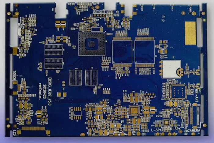
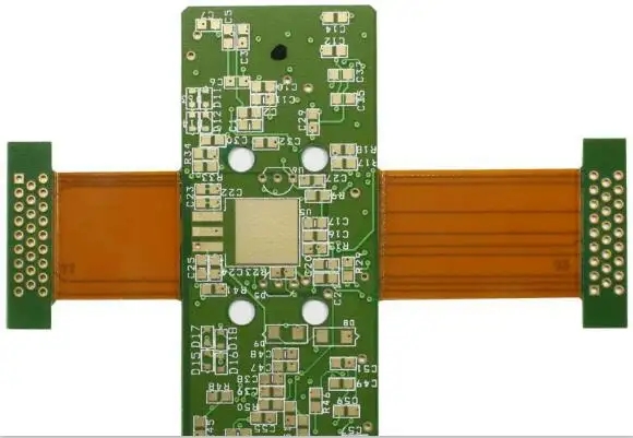
Printed circuit board can be divided into single panel, double panel, four layer board, six layer board and other multi-layer circuit boards according to the number of circuit board layers.
As PCB is not a general terminal product, the definition of its name is slightly confused. For example, the motherboard for personal computers is called the motherboard, but not the circuit board. Although there are circuit boards in the motherboard, they are not the same. Therefore, when evaluating the industry, they cannot be said to be the same. Another example: because there are integrated circuit parts loaded on the circuit board, the news media call it IC board, but in fact it is not the same as printed circuit board. The printed circuit board we usually refer to the bare board - that is, the circuit board without upper element devices.
At present, the defect rate of o/S in the inner layer of the circuit board is about 1.3%. The yield is only a reference for solving the problem priority, but there is no absolute operation rule. Because the production technology is difficult, I don't know if there is still much room for improvement. The quality improvement practices of other countries may not be effective for you, and the same digital level does not mean that the production capacity of circuit boards is the same. With the quality figures you have presented, the level is already quite high. If the statistical method is very accurate, the space for improvement seems limited.
Based on some advanced suggestions, shortcomings can be improved according to two basic principles. The first is to improve the problems that can be solved soon, and continue to improve the next problem after standardizing them. The second is to improve the problem of high proportion of shortcomings, because the effect of this approach will be more significant.
Generally, circuit board manufacturers will completely separate the defects of the inner layer from those of the outer layer, which is of course a clear way of analysis, because they have different impacts on products. However, the disadvantages of both are similar, because they are affected by the quality of exposure, development, etching and film removal
The impact of the situation. The inner layer of the circuit board is mostly made by the positive film process, while the outer layer of the circuit board is mostly made by the negative film process. Therefore, the two will have the opposite defect mode of short circuit. In addition, the outer layer of the circuit board needs to face multiple processing after completion, and these effects should also be included in the evaluation.
The famous saying of QC said, "Don't treat exceptions as problems. Only the projects with problems should be solved by technology.". Many phenomena may be the sequela of management. Most of these aspects can be self reviewed and improved without external demands. The above is for your reference.
Techniques for Reducing EMI of PCB
Nov 06,2022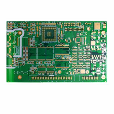


Just upload Gerber files, BOM files and design files, and the KINGFORD team will provide a complete quotation within 24h.