Detailed explanation of common PCB printing defects and solutions
In the SMT printing process, printing defects will inevitably occur. In the actual printing process, there are five kinds of defects: missed printing, bridging, collapse, tip pulling and offset. These printing defects are mainly affected by such factors as template, solder paste, scraper and printing process parameters.
Solder paste printing defect
1、 Common defects
(1) Misprinting: Misprinting is also called incomplete printing, mainly due to the blocking of the template mesh; The separation speed is too low; The opening of formwork is too small or the position is wrong; Solder paste viscosity is too small and other factors. If the separation speed is too low, the solder paste will not be off the screen well, which will not only make the pad not get enough solder paste, the printing is not complete, but also contaminate the template; If the viscosity of the solder paste is too small, the solder paste will not roll on the template during printing, so that the solder paste cannot completely fill the template mesh, causing insufficient solder paste deposition, slowing down the printing speed, increasing the scraper delay appropriately, so that the solder paste on the scraper can fully flow to the template, which can improve the rolling property of the solder paste.

(2) Bridging: Bridging is also called bridging, adhesion or tin bonding, mainly due to excessive printing pressure; The viscosity of solder paste is low; The steel mesh is not wiped clean; The formwork is too thick and the opening size is too large. The printing pressure can be reduced by modifying the printing process parameters; The viscosity of solder paste is too small, which is easy to flow and collapse, affecting the resolution and flatness of printing and causing bridging. Therefore, solder paste with high content of alloy solder powder can be selected.
(3) Collapse: the collapse is mainly due to the small hardness of the scraper; Solder paste viscosity is too low; The thickness of printing solder paste is too high; The formwork is not clean. The hardness of the scraper is too small, which will make the solder paste difficult to form. When demoulding, the printed shape of the solder paste cannot be maintained, and the appearance is vague. A hard scraper can be replaced; The collapse caused by low solder paste viscosity can be adjusted by increasing the content of alloy solder powder in the solder paste, reducing the particle size of alloy powder, and reducing the working environment temperature; If the thickness of printing solder paste is too high, it can be adjusted by adjusting the printing gap, selecting a thinner template, reducing the printing pressure, etc.
(4) Sharpening: poor separation of steel mesh is the main reason for sharpening; Poor printing clearance; The viscosity of solder paste is too high; It is caused by the unequal factors of the screen opening. Among them, the poor separation of the steel mesh will make it difficult to separate the solder paste from the template window, pollute the template, and form a pull point. The separation speed of the template should be readjusted; Poor printing clearance directly affects the thickness of printing solder paste. Especially when the template tension is large and the scraper pressure is not large, the increase of printing clearance will increase the thickness of printing. However, we usually do not increase the thickness of solder paste by increasing the printing clearance. Generally, the printing clearance is set to zero.
(5) Offset: offset is also called deviation, mainly due to excessive printing pressure; Steel mesh position offset; PCB size error, low repeated precision of printing machine and other factors. Among them, the position of the steel mesh is offset, which may be caused by the loose formwork, which needs to be re aligned; PCB size error may be caused by insufficient accuracy, so PCB with higher accuracy shall be selected.
2、 Solutions
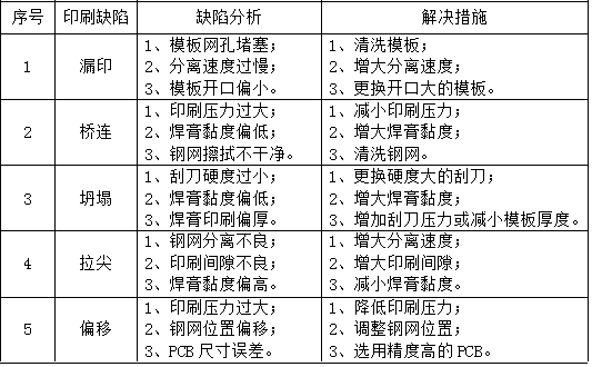
PCB manufacturers, PCB designers and PCBA processors will explain common PCB printing defects and solutions.


