
Professional PCB manufacturing and assembly
Building 6, Zone 3, Yuekang Road,Bao'an District, Shenzhen, China
+86-13410863085Mon.-Sat.08:00-20:00

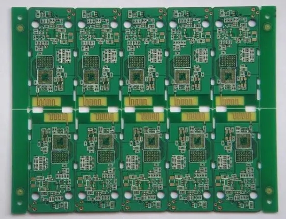
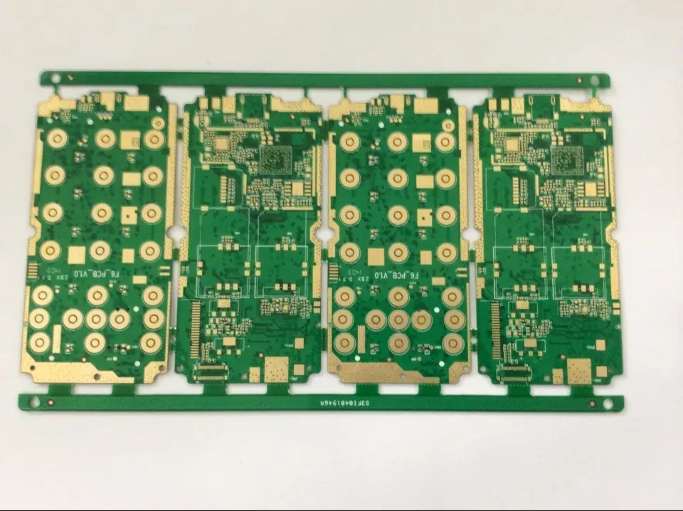
SMT placement order selection of steel two-sided component PCB
The circuit board manufacturer and circuit board designer will explain the SMT placement sequence selection of steel double-sided components PCB
SMT process: short for Surface Mount Technology, SMT surface mount technology is an electronic assembly technology that originated in the 1960s, was initially developed by IBM in the United States, and then gradually matured in the late 1980s. SMT technology is to install electronic components, such as resistors, capacitors, transistors, integrated circuits, etc. on printed circuit boards, and form electrical connections through lead soldering. The components used are also referred to as SMD (surface mount devices). The biggest difference between SMT and plug-in technology is that SMT surface adhesion technology does not need to reserve corresponding through holes for the pins of components, and the component size of surface adhesion technology is much smaller than that of plug-in packaging. This SMT technology can greatly reduce the volume of electronic products to achieve the purpose of thin and short, referred to as SMT process.
SMT placement order selection of steel two-sided component PCB
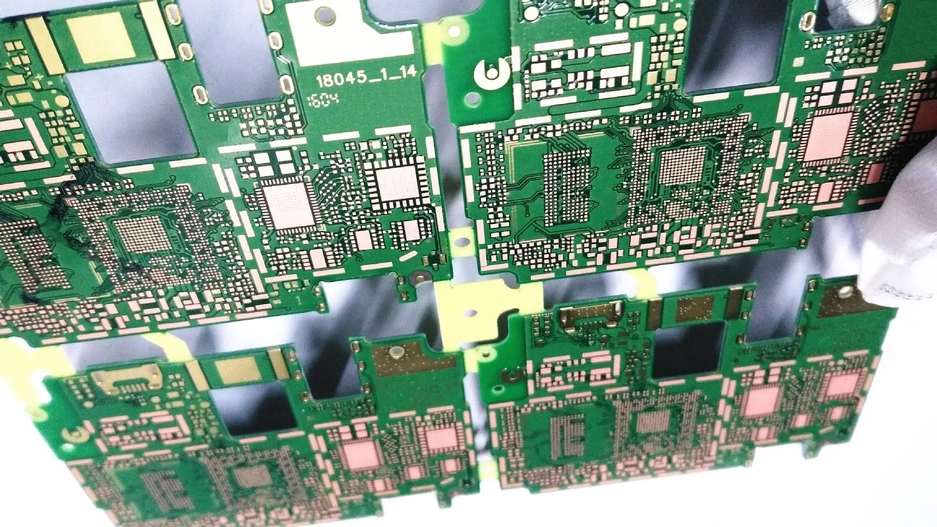
If the circuit board needs to be printed on both sides (side1, side2 or A, B), which side should be printed first? How to decide which side to play first? What are the decisive points? This problem is more complicated. Generally speaking, at the beginning of product design, it is necessary to decide which parts should be placed on the first side and the second side according to DFM (Design For Manufacturing) design specifications. It's just that sometimes things go against one's wishes. The factory may not be able to put forward any DFM suggestions.
First of all, when the parts on the first side of the board are finished, the parts on the second side will be turned over and put down, and then the parts on the second side will go through a high temperature reflow furnace together. If there are heavy parts on the bottom (the first side) at this time, when the parts on the second side go through the reflow furnace, they will easily fall down due to gravity and the possibility of solder paste re melting. So generally, the side with heavy parts will be placed on the second side to print.
Secondly, when there are BGA or LGA parts, it is recommended to place the parts on the second side, and only go through the reflow furnace once, for fear that the second pass will affect the parts dropping and solder reflow. If there are other fine pitch parts, due to the need for fine alignment, it is generally better to print the parts on the first side than on the second side. After the circuit board passes through the first reflow furnace, the board is easy to bend and deform due to the influence of temperature, which will cause offset of solder paste printing, and the amount of solder paste is not easy to control.
Of course, these are just the principles in SMT chip processing, and there are often exceptions. Because there are some antecedent limitations in the two-sided process, it is just to choose a step that has the least impact on the process and can optimize the quality.


Just upload Gerber files, BOM files and design files, and the KINGFORD team will provide a complete quotation within 24h.