
Professional PCB manufacturing and assembly
Building 6, Zone 3, Yuekang Road,Bao'an District, Shenzhen, China
+86-13410863085Mon.-Sat.08:00-20:00

Six PCB detection technologies and their advantages and disadvantages
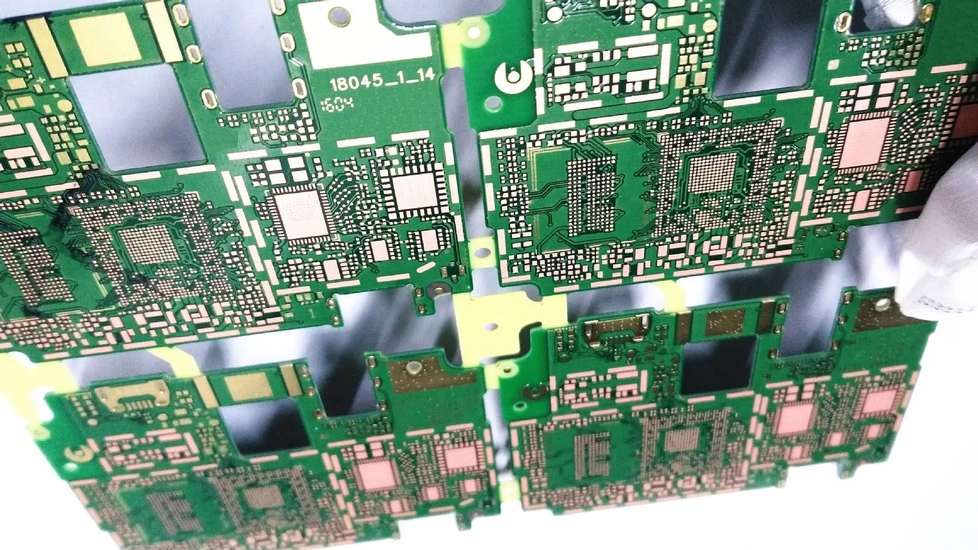
PCB detection is the "middle account of the three armies" for PCB manufacturing process quality. It is also the core competitive field of PCB manufacturers and plays a fundamental role in the entire PCBA processing process. At present, the main PCB inspection technologies at home and abroad are divided into two categories: optical inspection and electrical inspection, which specifically include PCB manual visual inspection, PCB online inspection (ICT), PCB function inspection (FCT), PCB active optical inspection (AOI), PCB active X-ray inspection (AXL, Automatic X-ray Inspection) and PCB laser inspection. There are a total of six inspection technologies.
1. PCB manual visual inspection
The magnifying glass or microscope is mainly used to manually identify the short circuit, open circuit and some appearance defects on the PCB, such as blistering, twisting, etc
[Advantages] Cost economy
[Disadvantages] The error correction rate is poor and the subjective deviation is great. As the line width and line spacing become narrower, this method has been gradually eliminated
2. PCB online detection (ICT)
ICT detection principle mainly simulates the electrical connection of PCB, so as to detect the main defects such as open circuit and short circuit of PCB through test points. ICT includes several test equipment such as Bed of Nails Tester and Flying Probe Tester.
[Advantages] Low test cost, easy programming and high defect coverage
[Disadvantages] Test fixture is specially made for PCB, which is relatively expensive and difficult to use
3. PCB function test (FCT)
Function testing is mainly to simulate the use of products, connect and program PCB boards through professional equipment, so as to truly reproduce the performance of products in use.
[Advantages] 100% ready to reproduce PCB performance
[Disadvantages] The design process is complex and costly, which is not suitable for most PCB production processes
4. PCB active optical inspection (AOI)
At present, the optical detection technology is relatively mature, which is mainly based on the optical principle, combined with computer and automatic control methods, to take pictures of PCB boards and compare them with the preset images and programs, so as to detect the problems in PCB board circuit connection extremely accurately.
[Advantages] High success rate of detection
[Disadvantages] The cost advantage is not very prominent, and the efficiency is moderate. Generally, a large number of testing equipment is required to cope with mass production
5. PCB active X-ray detection
X-ray detection is mainly used in high-precision and difficult processes, such as BGA and PoP process design. Its principle is to use X-ray irradiation projection, similar to manual X-ray photography, to detect the internal defects of PCB boards. It has good detection capability for blind hole embedding and other processes.
[Advantages] Adaptability to difficult detection
[Disadvantages] High cost, poor detection efficiency and high repair cost
6. PCB laser detection
The principle is to use laser beam to scan PCB, collect all measurement data, compare the data with the preset limit value of the system, and accurately feed back the deviation between PCB and design on the data level, so as to accurately find defects.
[Advantages] Suitable for mass production, high speed, and independent of fixture
[Disadvantages] The initial cost is very high, and professional personnel are required for maintenance and program setup
PCB detection technology is changing with each passing day, mainly to find a balance in efficiency, accuracy and cost. There are many detection equipment in the market, which can be used in different occasions to detect basic short circuit and open circuit defects easily. However, any PCB detection technology can not be separated from human management.


Just upload Gerber files, BOM files and design files, and the KINGFORD team will provide a complete quotation within 24h.