
Professional PCB manufacturing and assembly
Building 6, Zone 3, Yuekang Road,Bao'an District, Shenzhen, China
+86-13410863085Mon.-Sat.08:00-20:00

Causes of poor tin coating on lead-free tin spraying plate
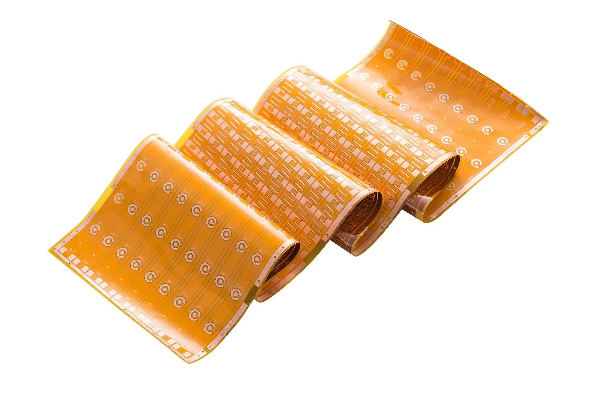
Lead free tin spraying plate
To tell the truth, sometimes I don't recommend using tin stencil for SMT processing, especially for double-sided SMT processing, because the defect rate is really high and it is not easy to overcome. It is believed that most friends who play with SMT process will first doubt whether it is solder paste (thickness, opening, pressure, etc. of steel mesh), solder paste over aging oxidation, SMD part foot oxidation, or the temperature curve of reflow soldering that is not adjusted properly when they encounter such SMD parts with poor tin eating.
I wonder if you have ever thought that most of the reasons for these solder defects may be the tin spraying thickness of the tin spraying plate. What you are familiar with before is that the thickness of the ENIG gold layer and nickel layer will cause solder problems, but will the thin tin layer of the tin spraying plate cause solder defects? Here are some book data collected for your reference.
Case Study on Unqualified Tin Coating of Lead free Soldering (HASL) (brief)
The cause of bad tin eating after reflow soldering on the second side of HASL board was analyzed. The results of metallographic section analysis show that copper and tin have been fully alloyed in places where tin solder pads are not used, and this copper tin alloy can no longer provide solderability.
The empty PCB boards of the same batch without soldering tin were inspected and sectioned for analysis. It was found that the tin coating on the soldered PCB pad without soldering had been exposed seriously. It can also be found that copper tin alloy is generated by slicing the blank PCB, and the measured thickness is about 2 μ m. Considering that the thickness of the alloy will increase later, it is speculated that the original tin spraying thickness should be 2 μ M, so it is inferred that the root cause is that the original tin coating thickness is too thin (2 μ M), so that copper tin alloying has been exposed to the surface of the solder pad, and there is not enough tin to be combined with solder paste, thus affecting the effect of solder pad eating.
How to deal with bad tin coating on one side of double-sided tin spraying plate (brief)
This should be an article that collates the opinions of all parties, but when it comes to the final analysis, it is mostly attributed to the thin thickness of tin spraying, resulting in poor soldering.
The tin spraying thickness is recommended to be at least 100u "(2.5 μ m) Above the large copper area, 200u "(5.0 μ m) Above QFP and peripheral parts, 450u "(11.4 μ m) Compared with BGA welding pad, it can solve the problem of solder rejection caused by reflow soldering on the second side. However, the thicker the tin spraying thickness is, the more unfavorable the thin leg parts are, and the problem of short circuit is easy to form.
In the PCB manufacturing process, the smaller the bonding pad is, the thicker the tin coating will be, which is easy to cause short circuit to the thin pin parts.
The longer the tin spraying plate is stored, the thicker the IMC (Cu6Sn5) will become, which will be more unfavorable for subsequent reflow soldering. Generally, the more flat the tin on the tin spraying plate is, the thinner the thickness will become.


Just upload Gerber files, BOM files and design files, and the KINGFORD team will provide a complete quotation within 24h.