
Professional PCB manufacturing and assembly
Building 6, Zone 3, Yuekang Road,Bao'an District, Shenzhen, China
+86-13410863085Mon.-Sat.08:00-20:00

In the process of PCB board reading design, the circuit schematic diagram is often drawn based on the real object. Therefore, mastering the method of converting the real object diagram of PCB board reading to the circuit schematic diagram will be the primary program for PCB board reading design.

Circuit board factory
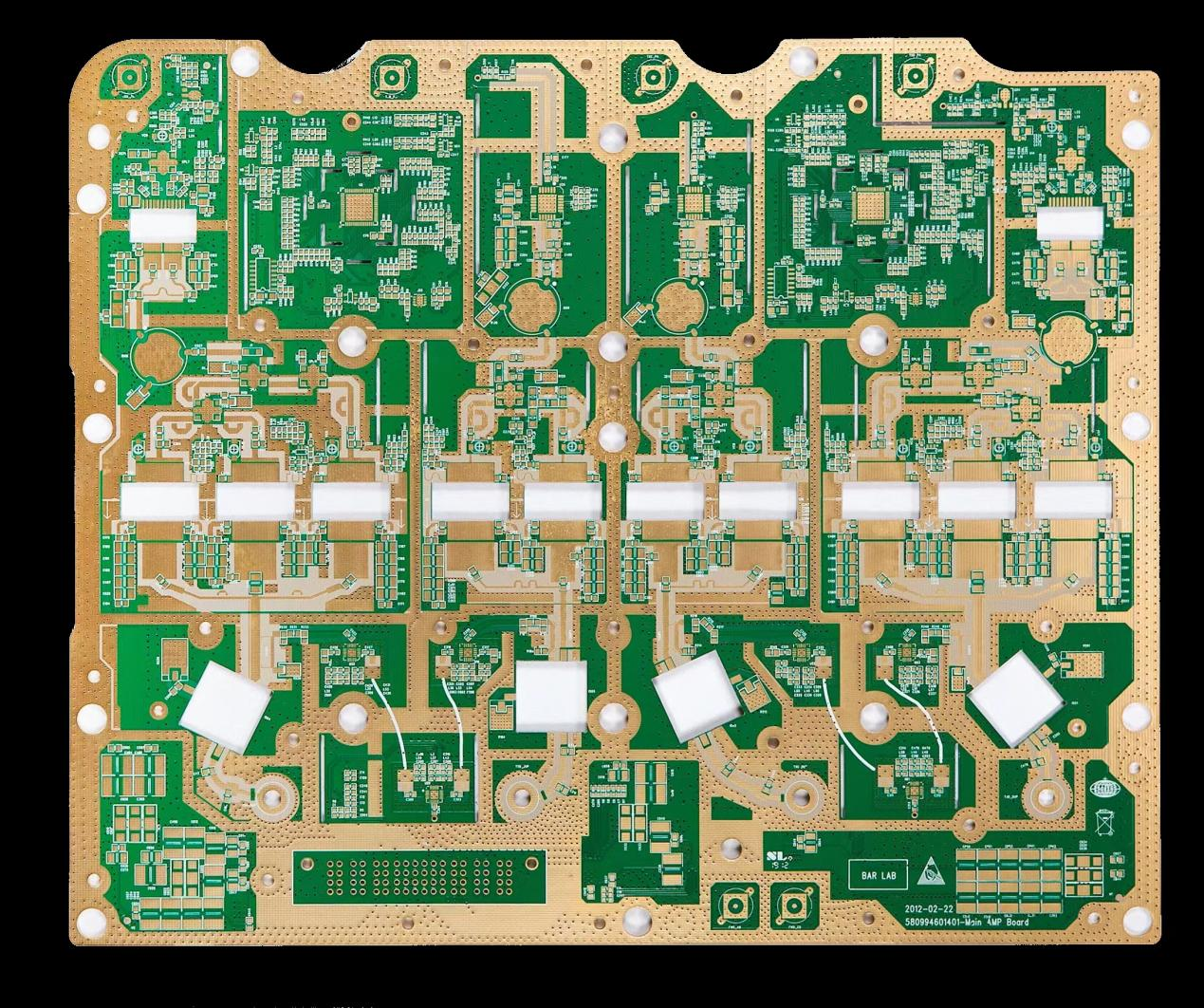
Circuit board factory restores circuit schematic diagram according to PCB circuit board
1. According to the experience given by the circuit board factory, it is necessary to select components that are large in size, have many pins and play a major role in the circuit, such as integrated circuits, transformers, transistors, etc., as drawing reference pieces, and then start drawing from each pin of the selected reference piece to reduce errors. Error prevention is also important in the manufacturing industry.
2. If the printed board is marked with component serial numbers (such as VD870, R330, C466, etc.), because these serial numbers have specific rules, the components with the same Arabic numerals in the first place after the English letters belong to the same functional unit, so they should be used skillfully when drawing. The correct differentiation of components of the same functional unit is the basis for drawing layout. There are many methods in the circuit board manufacturing methods of the circuit board factory that can be applied to restore the circuit schematic diagram.
3. If the serial number of the components is not marked on the printed board, it is better to number the components themselves to facilitate the analysis and proofreading of the circuit. In order to minimize the copper foil routing, the circuit board manufacturer generally centralizes the components of the same functional unit when designing the components arranged on the printed board. After finding the device that plays a key role in a unit, you can find other components of the same functional unit as long as you follow the steps.
4. According to the experience of the circuit board factory, correctly distinguish the ground wire, power wire and signal wire of the printed board. Taking the power circuit as an example, the negative terminal of the rectifier tube connected to the secondary of the power transformer is the positive terminal of the power supply, and a large capacity filter capacitor is generally connected between the rectifier tube and the ground wire. The capacitor shell has polarity marks. You can also find the power line and ground wire from the three terminal regulator pin. In order to prevent self excitation and interference when wiring printed boards, circuit board manufacturers generally set the widest copper foil for ground wires (high-frequency circuits often have large-area grounding copper foil), followed by power lines, and the narrowest copper foil for signal lines. In addition, in electronic products with both analog and digital circuits, the printed boards often separate their ground wires to form an independent grounding grid, which can also be used as a basis for identification and judgment.
5. In order to avoid excessive pin connections of components and parts, which may cause the wiring of the circuit diagram to cross and insert, resulting in the disorder of the drawing, a large number of terminal labels and grounding symbols can be used for power and ground wires. If there are many components, each unit circuit can be drawn separately and then combined together.
6. When sketching, it is recommended to use transparent tracing paper, and use a multi-color pen to draw ground wires, power lines, signal lines, components, etc. by color classification. When modifying, gradually deepen the color to make the drawing visual and eye-catching, so as to analyze the circuit.
7. Master the basic composition and classical drawing of some unit circuits, such as rectifier bridge, voltage stabilizing circuit, operational amplifier, digital integrated circuit, etc. First, these unit circuits are directly drawn to form the frame of the circuit diagram, which can improve the drawing efficiency.
8. When drawing the PCB circuit diagram, we should try to find the circuit diagram of similar products for reference, which will work twice with half the effort. Our circuit board factories and PCB manufacturers around the country rely on this method to restore the circuit schematic diagram.


Just upload Gerber files, BOM files and design files, and the KINGFORD team will provide a complete quotation within 24h.