
Professional PCB manufacturing and assembly
Building 6, Zone 3, Yuekang Road,Bao'an District, Shenzhen, China
+86-13410863085Mon.-Sat.08:00-20:00

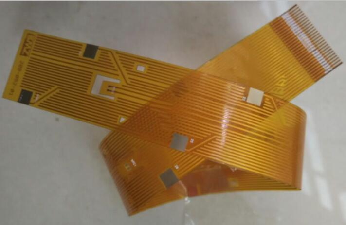
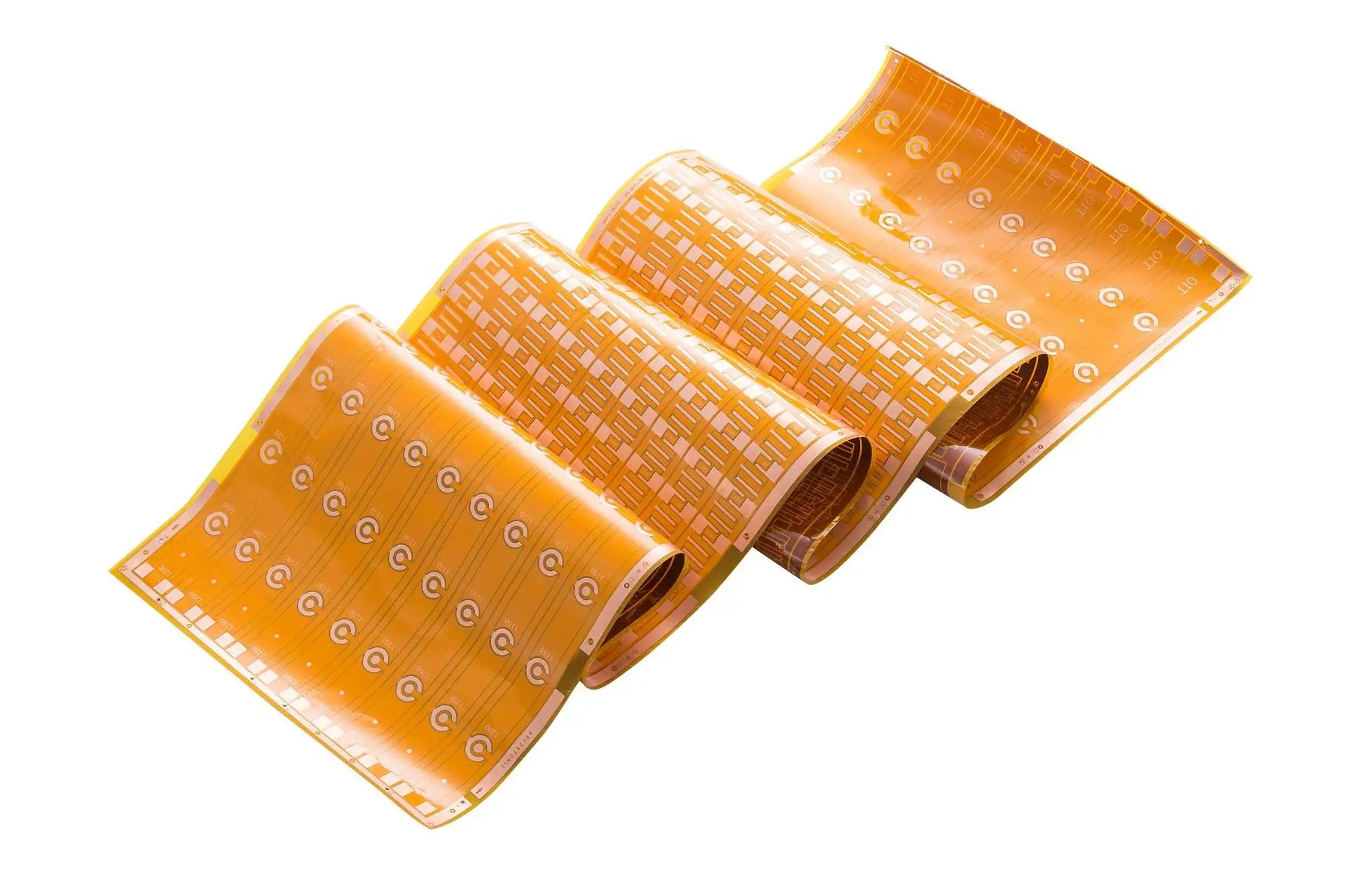
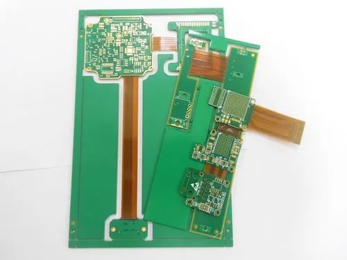
Flexible PCB is a highly reliable and excellent flexible printed circuit made of flexible insulating substrate such as polyimide or polyester film.
Flexible PCB

The basic standards for testing Flexible PCBs are as follows:
1. Appearance of substrate film surface:
The allowable defect range of substrate film surface appearance without conductor is listed in the table. It is not allowed to have other bumps, creases, wrinkles and foreign matters that affect the use.
2. Overlay appearance:
Defects of covering film and coating appearance: the allowable range is shown in the figure below, and no concave convex, crease, wrinkle and delamination affecting the use are allowed.
3. Deviation between connecting disc and covering layer:
As shown in the figure below, the allowable deviation e of the connecting disc and the covering layer is less than ± 0.3 mm when the overall dimension is less than 100 mm, and less than ± 0.3% when the overall dimension is more than 100 mm.
4. Flow penetration of binder and coating:
As shown in the figure below, the flow permeability f of the adhesive and the covering coating shall be less than 0.2mm. However, the minimum ring width g ≥ 0.05mm must be met at the connecting plate plus the covering layer deviation and punching deviation.
Discoloration of the conductor under the coating must still meet the requirements of voltage resistance, bending resistance, bending resistance and welding resistance after 96 hours of humidity resistance test at 40 ℃ and 90% humidity.
5. Holiday of coating:
As shown in the figure below, the missed coating of the coating layer shall be tested according to the solderability requirements, and the conductor of the missed coating part of the coating layer shall not be pasted with tin.
6. Poor electroplating combination:
The coating is not allowed to be layered, as shown in the figure below. The width of the coating where it is poorly bonded is W1, the length is L, and the width of the conductor after processing is W. Moreover, the poor coating bonding must not damage the reliability of the contact area.
The above are the basic standards for Flexible PCB testing


Just upload Gerber files, BOM files and design files, and the KINGFORD team will provide a complete quotation within 24h.