
Professional PCB manufacturing and assembly
Building 6, Zone 3, Yuekang Road,Bao'an District, Shenzhen, China
+86-13410863085Mon.-Sat.08:00-20:00

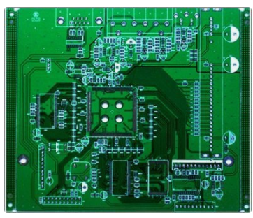
The following is an analysis of PCB negative deformation in PCB process
1、 The causes and solutions of film deformation are as follows:
reason:
(1) Temperature and humidity control failure
(2) The temperature rise of the exposure machine is too high
resolvent:
(1) Generally, the temperature is controlled at 22 ± 2 ℃ and the humidity is 55% ± 5% RH.
(2) Exposure machine with cold light source or cooling device and continuous replacement of backup film

2、 Process method of PCB negative deformation correction:
1. Under the condition of mastering the operation technology of the digital programming instrument, first install the negative film to compare with the drilling test plate, measure its length and width, lengthen or shorten the hole position according to the size of the deformation on the digital programming instrument, and use the drilling test plate after lengthening or shortening the hole position to match the deformed negative film, so as to avoid the tedious work of splicing the negative film, and ensure the integrity and accuracy of the graphics. This method is called "hole location change method".
2. In view of the physical phenomenon that the negative film changes with the change of ambient temperature and humidity, take out the negative film in the sealed bag before copying the negative film, and hang it in the air for 4-8 hours under the working environment to deform the negative film before copying, so that the deformation of the copied negative film will be very small. This method is called "hanging in the air method".
3. For graphics with simple lines, large line width and spacing, and irregular deformation, the deformed part of the negative film can be cut off and compared with the hole position of the drilling test plate, and then copied, which is called "splicing method".
4. This method is called "pad overlap method", which uses holes on the test board to enlarge the pad to remove heavy and deformed circuit pieces to ensure the minimum ring width technical requirements.
5. This method is called "mapping method", in which the figures on the deformed negative film are scaled up and remapped for plate making.
6. The camera is used to enlarge or reduce the deformed figure, which is called "photographic method".
3、 Precautions for relevant methods:
1. Splicing method:
Application: The PCB circuit is not too dense, and the film deformation of each layer is inconsistent; It is especially suitable for the deformation of resistance welding negative film and multilayer power supply layer negative film;
Not applicable: negative film with high wire density, line width and spacing less than 0.2mm;
Precautions: The conductor shall be cut as little as possible without damaging the bonding pad. Pay attention to the correctness of the connection relationship of PCB boards when editing after splicing copies.
2. Change hole location method:
Application: The deformation of each layer of negative film is consistent. This method is also applicable to films with dense lines;
N/A: The negative film has uneven deformation, especially local deformation.
Precautions: After using the programmer to lengthen or shorten the hole position, the hole position exceeding the tolerance shall be reset.
3. Hanging method:
Applicable; Negative film that has not been deformed and prevented from deformation after copying;
Not applicable: deformed negative film.
Precautions: Hang the negative film in a ventilated and dark (safe) environment to avoid pollution. Ensure that the temperature and humidity of the hanging place are consistent with that of the operation place.
4. PCB pad overlap method:
Applicable: the graphic lines are not too dense, and the line width and spacing are greater than 0.30mm;
Not applicable: In particular, users have strict requirements on the appearance of printed circuit boards;
Note: The pad is elliptical after overlapping copies. Halo and deformation of line and disk edges after overlapping copy.
5. Photographic method:
Application: The deformation ratio in the length and width directions of the negative film is consistent. When it is inconvenient to drill the test plate again, it is only applicable to silver salt negative film.
N/A: PCB negative is deformed inconsistently in the length and width directions.
Precautions: The focus should be accurate when taking pictures to prevent line deformation. There is a lot of film loss. Generally, you need to debug many times to get a satisfactory PCB circuit pattern.
In a word, this paper is mainly about the analysis of PCB negative deformation in PCB process
FPC knowledge and application of FPC soft board
Nov 02,2022


Just upload Gerber files, BOM files and design files, and the KINGFORD team will provide a complete quotation within 24h.