
Professional PCB manufacturing and assembly
Building 6, Zone 3, Yuekang Road,Bao'an District, Shenzhen, China
+86-13410863085Mon.-Sat.08:00-20:00

The copper free pores of the gradually thinner type have a common feature, that is, the copper layer in the pores gradually thins from the hole mouth to the hole center until the copper layer disappears. The details are as follows: Some customers wrongly judge that there is no copper in this type of hole as follows: 1. The ability of tin polish deep plating (displacement) is poor, so they call tin
The copper free pores of the gradually thinner type have a common feature, that is, the copper layer in the pores gradually thins from the hole mouth to the hole center until the copper layer disappears. The details are as follows:
Some customers misjudged that there was no copper in this type of hole as follows:
1. Poor tin plating (displacement) ability of tin polish and poor tin calling;
2. PTH is abnormal and no copper is deposited in the hole;
3. The deep plating ability of copper plating is poor.
In practical production, copper free tapered holes are common. The reason is that the conductive substrate (plate electroplated copper or thick copper layer) has an inhibitor layer that hinders copper electroplating. The generation and prevention of this coating are analyzed below.
During the next process of circuit development of sheet metal copper or heavy copper, the ink that is not cross-linked and polymerized on the PCB surface is dissolved in the developing solution, and the developing solution containing ink macromolecules is sprayed onto the PCB surface and holes again by the circulating pump. At this time, if the subsequent pressure water washing (including water quality) is not enough to wash the residues of ink macromolecules on the PCB surface and holes, Then the residual ink macromolecular compound will reverse stick on the hole wall to form a thin layer of barrier coating. The more it reaches the center of the hole, the worse the cleaning effect will be. The greater the probability of the barrier coating, especially the small holes. (The multi-stage washing of the developing section is just a process of continuously diluting the residue, so as to dilute the residue as much as possible.).
After understanding that the polymer anti adhesion coating is the culprit that causes the thin copper layer in the hole, the focus of the problem is to ensure the cleaning effect in the hole to remove the anti adhesion coating. Suiting the remedy to the case can cure the root cause.
In addition, the premise of dealing with practical problems is to face up to and respect the existing production conditions of customers, such as: PCB circuit and PCB solder resistance, dry film and wet film sharing the developer, and water washing flow is limited by environmental protection.
Some customers had hoped that the micro etching amount of the enlarged drawing could remove the resistance coating in the hole, but unfortunately, it did not help. Instead, excessive micro etching caused no copper in the hole. The correct solution should be to strengthen the maintenance of the developing dry process, and select acid degreaser with excellent degreasing effect for the graphic and electrical pretreatment.
EC-51 acid degreaser can cooperate with customers to solve the problem of copper free in such holes where the copper is gradually thinner from the orifice to the center of the hole. The correct use of EC-51 acid degreaser requires the following precautions:
1. EC-51 requires slightly strict water washing, which requires sufficient water washing. The copper cylinder and nickel cylinder may have more foam because the wetting agent contained in it is not clean.
2. EC-51 is specially designed for PCB wet film. If there is no nickel or copper plating in the hole, it can be solved after EC-51 treatment. For thin wire pitch dry film, the amount of cylinder opening shall be appropriately reduced, and the content of EC-51 shall be controlled to 4% to prevent the excessive content of degreaser from attacking the dry film line edge and causing dog tooth shaped coating. In addition, EC-51 is also good for copper free dry film tapered holes.
3. Winter is a time of high incidence of such problems (due to low temperature and poor water washing performance). The most effective way to improve the oil removal effect is to increase the temperature (the increase in concentration contributes little, but also increases the water washing pressure). The temperature is generally controlled at 30-35 ℃. Too low temperature is not conducive to ensuring the oil removal effect; Excessive temperature is prone to attack PCB ink with degreaser, which leads to infiltration. In the manual line, the manual swing and filter shall also be used to ensure the penetration of the liquid medicine in the hole.
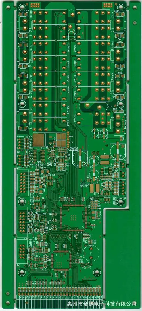
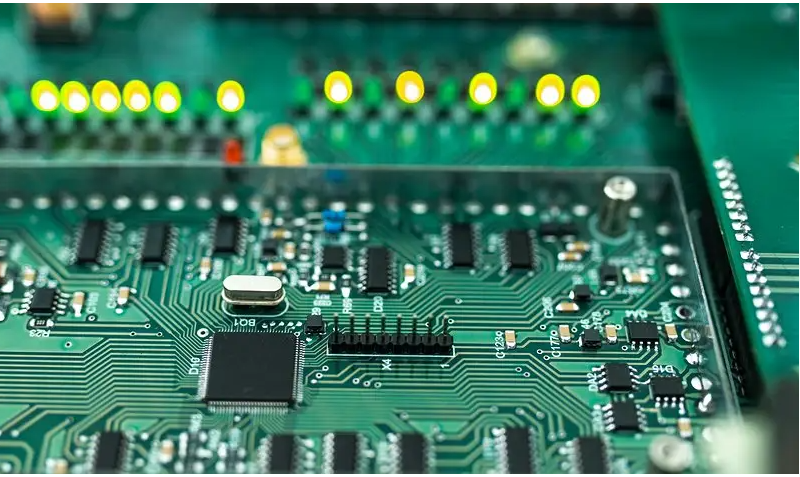
Main reasons for copper rejection of PCB
Nov 01,2022


Just upload Gerber files, BOM files and design files, and the KINGFORD team will provide a complete quotation within 24h.