
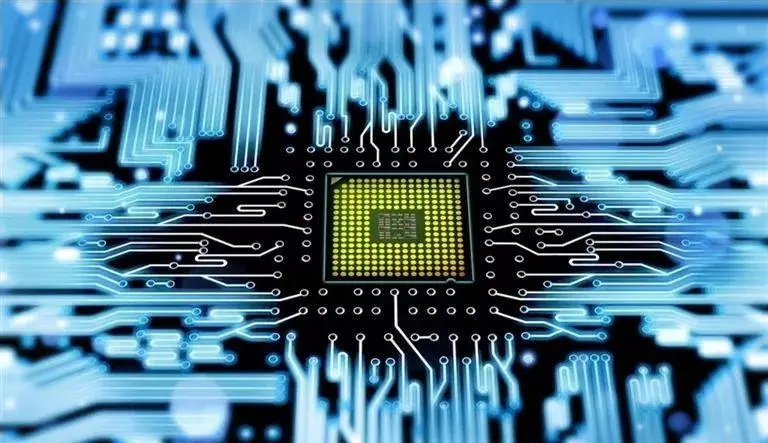
Professional PCB manufacturing and assembly
Building 6, Zone 3, Yuekang Road,Bao'an District, Shenzhen, China
+86-13410863085Mon.-Sat.08:00-20:00

The copper wire of PCB falls off (also known as copper throwing). PCB manufacturers say it is a laminate problem and require their production plants to bear the bad losses. According to my years of experience in handling customer complaints, the common reasons for copper rejection in PCB plants are as follows:
1、 PCB factory process factors:
The copper foil is excessively etched. The electrolytic copper foil used in the market is generally single-sided galvanized (commonly known as ashing foil) and single-sided copper plated (commonly known as reddening foil). The common copper rejection is generally more than 70um galvanized copper foil. The reddening foil and the ashing foil below 18um have basically no batch copper rejection. When the customer's circuit has designed the etched line, if the copper foil specification has changed but the etching parameters have not changed, the copper foil will stay in the etching solution for a long time. As zinc is a kind of active metal, when the copper wire on PCB is immersed in etching solution for a long time, it will inevitably lead to excessive side erosion of the circuit, resulting in the complete reaction of the zinc layer on the back of some thin circuits and separation from the substrate, that is, the copper wire falls off. Another situation is that there is no problem with PCB etching parameters, but after etching, the copper wire is also surrounded by the residual etching solution on the PCB surface due to poor water washing and drying. If the copper wire is not treated for a long time, it will also cause excessive side etching of the copper wire and copper throwing. This situation is generally manifested as concentrated on the thin line road, or in wet weather, similar defects will appear on the entire PCB. Peel off the copper wire to see that the color of its contact surface with the base layer (the so-called roughening surface) has changed, which is different from the color of the normal copper foil. What you see is the color of the original copper at the bottom layer, and the peeling strength of the copper foil at the thick line is also normal.
2. In PCB process, local collision occurs, and the copper wire is separated from the substrate by external mechanical force. This defect is characterized by poor positioning or orientation, and the detached copper wire will have obvious distortion, or scratches/impact marks in the same direction. Peel off the copper wire at the defective part and look at the rough surface of the copper foil. It can be seen that the color of the rough surface of the copper foil is normal, there is no side corrosion, and the peeling strength of the copper foil is normal.
3. The PCB circuit design is unreasonable. If the circuit is designed too thin with thick copper foil, it will also cause excessive etching of the circuit and copper throwing.
2、 Reasons for laminate manufacturing process:
Under normal circumstances, as long as the high temperature section of the laminate is hot pressed for more than 30min, the copper foil and the prepreg will be basically bonded, so the bonding will not affect the bonding force between the copper foil and the substrate in the laminate generally. However, in the process of laminating and stacking, if PP is polluted or the rough surface of the copper foil is damaged, the bonding force between the copper foil and the substrate after laminating will also be insufficient, resulting in positioning (only for large plates) or sporadic copper wire falling off. However, there will be no abnormality in the peeling strength of the copper foil near the measuring line.
3、 Reasons for raw materials of laminate:
1. It is mentioned above that ordinary electrolytic copper foil is a PCB product that has been galvanized or coppered with rough foil. If the peak value is abnormal during the production of rough foil, or the coating crystal branch is poor during galvanizing/copper plating, resulting in insufficient peeling strength of the copper foil itself. When the defective foil is pressed into a PCB and is inserted in the electronics factory, the copper wire will fall off under the impact of external forces. Such poor copper throwing will not cause obvious side erosion after peeling off the copper wire to see the rough surface of the copper foil (i.e. the contact surface with the base material), but the peeling strength of the entire copper foil will be very poor.
2. Poor adaptability of PCB copper foil and resin: some laminates with special properties, such as HTg sheet, are now used. Due to different resin systems, the curing agent used is generally PN resin. The resin molecular chain structure is simple, and the degree of crosslinking during curing is low. Therefore, copper foil with special peak value must be used to match it. When the copper foil is used in the production of the laminate, it does not match the resin system, resulting in insufficient peeling strength of the metal foil on the sheet, and poor copper wire falling off during the plug-in.
Interconnection mode of PCB
Nov 01,2022


Just upload Gerber files, BOM files and design files, and the KINGFORD team will provide a complete quotation within 24h.