
Professional PCB manufacturing and assembly
Building 6, Zone 3, Yuekang Road,Bao'an District, Shenzhen, China
+86-13410863085Mon.-Sat.08:00-20:00

Application field and structure of multilayer circuit board
Generally, the fabrication method of multilayer board is to make the inner layer pattern first, then make a single or double sided substrate by printing and etching, and incorporate it into the designated interlayer, and then heat, pressurize and glue it. As for the later drilling, it is the same as the plating through hole method of double-sided board. It was invented in 1961.
1 Application field of multilayer circuit board
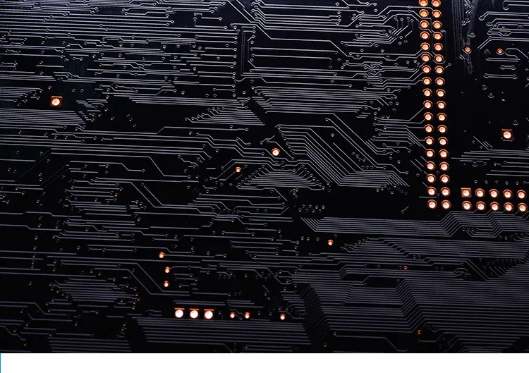
Multilayer PCBA boards generally focus on electroplated through-hole. The number of layers, plate thickness, and hole location configuration vary with the circuit density. The classification of specifications and contents is based on this. Rigid Flex multipurpose i military, aerospace and instrument equipment is rare in general consumer electronics products, so it will not be discussed in detail. Under the premise that electronic products tend to be multi-functional and complex, the contact distance of integrated circuit components will be reduced, and the speed of signal transmission will be relatively improved, followed by an increase in the number of wiring and a local reduction in the length of wiring between points. These require high-density circuit configuration and microporous technology to achieve the goal. Wiring and jumper are basically difficult to achieve for single and double sided boards, so the circuit board will move towards multi-layer; Moreover, due to the continuous increase of signal lines, more power supply layers and ground layers have become necessary means for design, which has promoted the popularization of multilayer printed circuit boards.
The printed circuit board establishes the metal layer in an independent circuit layer, so the longitudinal connection between layers is indispensable. In order to achieve the purpose of interlayer connection, it is necessary to use drilling method to form a path and form a reliable conductor on the hole wall to complete the connection of power or signals. Since through-hole electroplating was proposed, almost all multilayer circuit boards have been produced by this method|
The increased density circuit board is fabricated by layer adding mode, which is formed by forming small holes on the dielectric material in the way of laser or J light sensing, and then conducting by electroplating. Some manufacturers fill the connecting holes with conductive adhesive to achieve continuity, such as ALIVH and B2it developed in Japan.
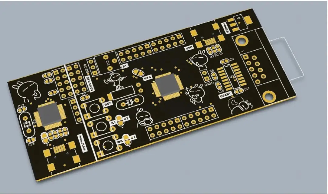
Multilayer printed circuit boards can have single-sided, double-sided, 4-layer, 6-layer, 8-layer structures depending on the number of layers of the circuit. As for the recently mentioned high-density circuit board, because the usual production method is to build a core hard board in the center, and on this basis, grow layers on both sides. Therefore, there are two common names. One is to use the number of hard board layers in the center as the first number, and the number of wire layers added on both sides as the other number. Therefore, there are so-called 4+2, 2+2, 6+4 descriptions. However, another name may make it easier for people to understand the actual situation. Because most multi-layer circuit board designs explore symmetric design, we will explore the names of 1+4+1, 3+6+3, etc. At this time, if someone says that a 2+4 structure may be an asymmetric structure, we must confirm it.


Just upload Gerber files, BOM files and design files, and the KINGFORD team will provide a complete quotation within 24h.