
Professional PCB manufacturing and assembly
Building 6, Zone 3, Yuekang Road,Bao'an District, Shenzhen, China
+86-13410863085Mon.-Sat.08:00-20:00

Will BGA short circuit be caused by offset of solder mask printing of circuit board?
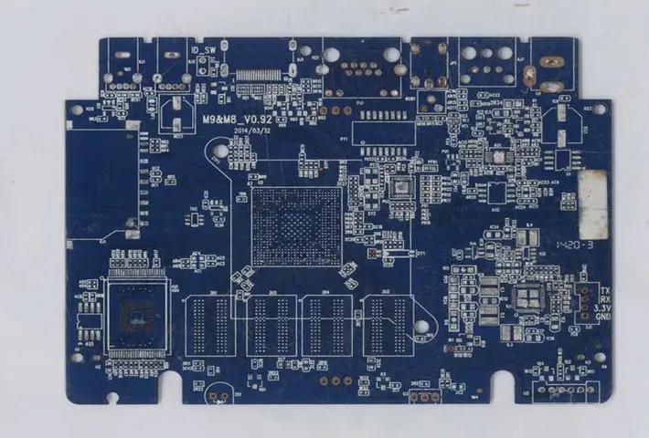
The company is working on a new project recently. RD's requirements for board layout are becoming more and more strict, because the boards are getting smaller and smaller, and the associated requirements for the size of solder mask are also relatively reduced. However, the manufacturer's manufacturing process capability cannot keep up with it. Those who have the ability to say that they need to increase the price. When they hear that they need to increase the price, everyone starts to back down and continue to use the manufacturing process of the existing PCBA board factory. As a result, the offset of solder mask printing exceeds the pad/pad.
What problems will be caused by offset of solder mask printing?
If the pad/pad of BGA is offset, the pad of BGA solder ball will become smaller, and eventually lead to solder short. How can the smaller pad cause short circuit instead? The original opening on the steel plate is fixed, that is, the amount of solder paste for the same opening on the steel plate is fixed in theory. If the pad size of each circuit board BGA is the same, the steel plate can be given an appropriate opening size and amount of solder paste according to the actual pad size. However, if different batches of circuit boards, some pads maintain the original size, but some pads shrink, but the amount of solder paste remains the same, It will become a phenomenon of overflow caused by too much solder paste. In severe cases, it will overflow to the adjacent solder pad, forming a solder short circuit.
But how can the pad (pad) become smaller?
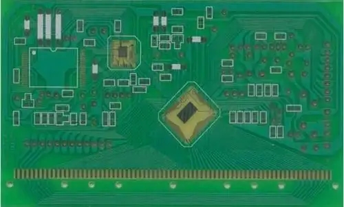
It's like wearing a head covering only exposes two eyes. If the head covering is not in the correct position and is slightly biased, the eyes will be covered by the head covering, covering half of the eyes. Eyes can be imagined as welding pads, while the solder mask is a headpiece. Some people may see that the article is still unclear, so I'm going to argue that the Solder Mask is green paint! Do you understand! If you don't understand, just take out the board and look at the large green area! These green paints will cover the copper foil and lines that do not need to be exposed on the circuit board to avoid unnecessary contact short circuit or oxidation. (Note: some boards will be printed in black and red, but most of them are green)
Because the company's new circuit board design focuses on the tolerance of the solder mask layer at+/- 1mil (+/-0.0254mm), but the process capacity of the solder mask layer of the board factory is+/- 2mils (+/-0.05mm), so the solder mask layer with actual printing deviation will cover the original exposed solder pad, making the original exposed solder pad smaller, thus causing the above problems. Another reason is that in order to prevent the occurrence of HIP, we print more solder paste on the outer ring of BGA, so the solder pads with short circuit are almost concentrated on the outer ring solder balls of BGA. (Related reading: How to solve the problem of HIP (Head In Pillow) faulty soldering of BGA solder balls)
Next solution:
1. The circuit board factory is required to modify the hole position and size of the solder mask of the problematic solder pad locally. In principle, it is required that all the solder pads under BGA should have the same size.
2. Reopen the steel plate (stencil) to narrow the opening of BGA outer ring welding pad that is prone to short circuit, so as to reduce the amount of solder paste printing.
What can the solder paste tester do
Oct 31,2022


Just upload Gerber files, BOM files and design files, and the KINGFORD team will provide a complete quotation within 24h.