
Professional PCB manufacturing and assembly
Building 6, Zone 3, Yuekang Road,Bao'an District, Shenzhen, China
+86-13410863085Mon.-Sat.08:00-20:00

concept
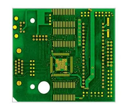
Reproduction of goods is called processing; entrusted processing of goods refers to the business in which the entrusting party provides raw materials and main materials, and the entrusting party manufactures the goods according to the requirements of the entrusting party and collects processing fees. PCB processing is the reproduction of circuit boards according to customer requirements.
PCB processing flow
Cutting principle: Cut the large material into small pieces according to the size required by MI
Inner layer: paste dry film or printing oil, expose, develop, etch and strip film. The inner layer corrosion inspection is a process of pattern transfer. By using film negatives, ink/dry film and other media under the irradiation of ultraviolet light, the customer needs The circuit pattern is made on the inner layer substrate, and then the unnecessary copper foil is etched away, and finally the conductive circuit of the inner layer is formed.
Pre-treatment: Grinding the inner layer of the inner layer of the dry film, inner layer etching and internal inspection + roughening the surface of the copper plate, in order to increase the bonding force between the plate surface and the drug film + cleaning the surface of the plate, remove the debris on the surface of the plate, and the coverage of the dry film and copper foil Coverage of ink and copper foil
Pressing process: browning, arranging, pressing, X-RAY punching, hole and gong
Drilling process: The role of drilling: to produce a channel on the circuit board that allows the post-process to complete the connection between the upper and lower parts of the circuit board or the conductive properties between the middle circuit layers

Wet process: copper sinking - outer layer dry film - pattern plating or plate plating - outer layer - etching plate - outer layer - corrosion inspection
Immersion copper function: Deposit a conductive copper layer on the insulating hole wall of the circuit board to conduct the connection with the inner layer circuit.
Outer layer dry film: paste dry film exposure development
Pattern electroplating or board electroplating: Function: Increase the copper thickness of the circuit board hole\line\surface, so that it can meet the customer's requirements.
Outer layer etching: Stripping: Use strong alkali to dissolve or peel off the dry film to peel off or dissolve the unwanted dry film from the board
Etching the board: Use the oxidative properties of the divalent cupric ammonium complex and ion to etch away the unwanted copper from the board
Tin stripping: The nitric acid in the tin stripping water can react with tin to dissolve the tin layer to remove the tin from the board
Outer layer inspection: AOI&VRS captures the image of the PCB circuit board through CCD scanning, uses the computer to compare it with the CAM standard graphics and processes the design specification logic, marks the bad points on the circuit board and transmits the coordinates of the bad points to VRS for final confirmation
The location of the bad spot.
Wet film process: The main process stations are: printing a layer of photosensitive ink on the circuit board surface of the outer circuit board that has been formed, so as to cure it, so as to protect the outer layer and insulation of the circuit board. Pretreatment Grinding plate, ink printing, oven exposure development, character printing
Surface treatment process: mainly according to the customer's requirements, the exposed copper surface of the circuit board is processed with a layer of processing.
The main treatment processes are: Spray tin: use the hot air welding process to spray a layer of solderable tin surface on the copper surface.
Immersion Tin: Using the principle of chemistry, tin is deposited on the board by chemical treatment.
Immersion Silver: Using chemical principles to deposit silver on the board through chemical principles.
Immersion Gold: Using chemical principles to deposit gold on the board through chemical principles.
Gold plating: Using the principle of electroplating, the gold is plated on the board by current and voltage control.
Anti-oxidation: Using the principle of chemistry, an anti-oxidation chemical is applied to the board surface
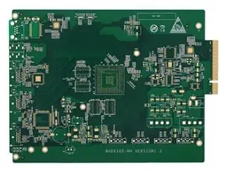
Forming process: It is mainly to process an already formed circuit board into the size and shape required by the customer according to the requirements of the customer.
Open and short circuit test inspection: mainly to check the open circuit and short circuit inspection of the line, and to check the quality of the board surface with eyes.
Packing and shipping: The boards that have passed the inspection will be packaged and finally shipped to customers.
important raw materials
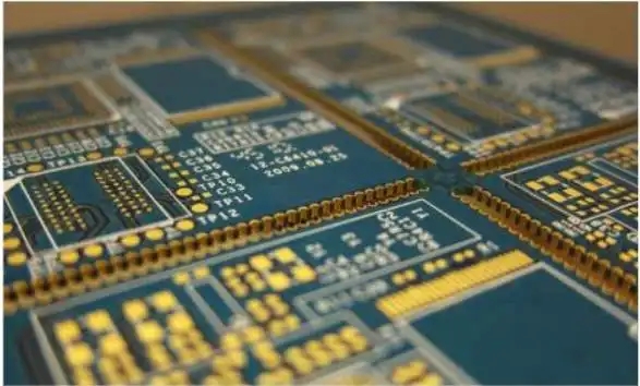
substrate
The original material of the PCB board is the copper clad substrate, referred to as the substrate. The base plate is a resin board with copper on both sides. Now the most commonly used plate code is FR-4. FR-4 is mainly used for electronic products of computer, communication equipment and other grades. Requirements for the sheet: one is the flame resistance, the other is the Tg point, and the third is the dielectric constant. The circuit board must be flame-resistant, it cannot burn at a certain temperature, it can only soften. The temperature point at this time is called the glass transition temperature (Tg point), and this value is related to the dimensional stability of the PCB board. In advanced applications, customers sometimes specify the Tg point of the sheet. The dielectric constant is a quantity that describes the electrical properties of a substance. In high-frequency lines, the dielectric loss (PL) of a signal is related to the substrate material, specifically proportional to the square root of the dielectric constant of the medium. The greater the loss of the medium, the greater the effect of absorbing high-frequency signals and converting them into heat, resulting in the inability to transmit signals effectively.
In addition to FR-4 resin substrates, phenolic paper substrates are also widely used in simpler applications such as televisions and radios.
Let's take a look at the composition of the substrate. The substrate is composed of base material and copper foil. The FR-4 base material is resin and glass fiber cloth, and the glass fiber cloth is the fabric of glass fiber. The glass fiber cloth is dipped in liquid resin, and then pressed and hardened to obtain the base material. In polymer chemistry, the state of the resin is divided into three states: a-stage, b-stage, and c-stage. There is no close chemical bond between the resin molecules in the a-stage, and it is in a fluid state; in the b-stage, the molecules and the There are not many chemical bonds between molecules, and it will soften under high temperature and high pressure, and then become c-stage; c-stage is the most stable state of the chemical structure of the resin, which is solid, and the chemical bonds between molecules increase, and the physical and chemical properties are very stable. The circuit board substrates we use are made of b-stage resin. The substrate is to hot press the base material in b-stage and copper foil together. At this point the resin is in a stable c-stage.
copper foil
Copper foil is a conductor that forms wires on a substrate. There are two methods of manufacturing copper foil: rolling and electrolysis.

Calendering is to press high-purity copper material into a copper foil with a thickness of only 1 mil (equivalent to 0.0254mm) like a dumpling wrapper. The production method of electrolytic copper foil is to use the principle of electrolysis, using a huge rolling metal wheel as the cathode, and CuSo4 as the electrolyte, so that pure copper is continuously precipitated on the rolling metal wheel to form copper foil. The specification of copper foil is thickness, and the thickness of copper foil commonly used in PCB factories is between 0.3 and 3.0 mils.
PP
PP is an indispensable raw material in the production of multi-layer boards, and its function is the adhesive between layers. Simply put, the substrate sheet at the b-stage is called PP. The specifications of PP are thickness and glue (resin) content.
dry film
Photosensitive dry film is referred to as dry film, and its main component is a resinous substance that is sensitive to a specific spectrum and undergoes a photochemical reaction. A practical dry film has three layers, with the photosensitive layer sandwiched between two layers of protective plastic film above and below. According to the chemical characteristics of photosensitive substances, there are two types of dry films, photopolymerization and photodecomposition. Photopolymerizable dry film will harden when irradiated with light of a specific spectrum, changing from water-soluble to water-insoluble, and photodegradable is just the opposite.
Solder mask
Solder resist is actually a solder resist, a liquid photosensitive material that has no affinity for liquid solder. Like photosensitive dry film, it will change and harden under the irradiation of a specific spectrum of light. When used, the solder mask should be mixed with the hardener. Solder mask is also called ink. The color of the PCB board we usually see is actually the color of the solder mask.
negative
The negatives we are talking about are similar to photographic negatives, and they are all materials that use photosensitive materials to record images. The customer transmits the designed circuit diagram to the PCB factory, and the work station in the CAM center outputs the circuit diagram, but not through a common printer, but a light plotter (Plotter, Figure 1), and its output medium is the negative film, also called film (film). Where the film is exposed, it is black and opaque, whereas it is transparent. The role of the negative film in the PCB factory is pivotal. All using the principle of image transfer, to achieve something on the substrate, it must first be turned into a negative film.


Just upload Gerber files, BOM files and design files, and the KINGFORD team will provide a complete quotation within 24h.