
Professional PCB manufacturing and assembly
Building 6, Zone 3, Yuekang Road,Bao'an District, Shenzhen, China
+86-13410863085Mon.-Sat.08:00-20:00

Common quality defects and solutions of reflow soldering in PCB engineering
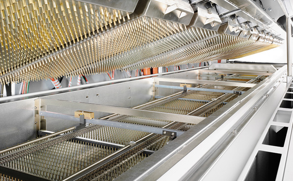
The quality of reflow soldering is affected by many factors. The most important factors are the temperature curve of reflow soldering furnace and the composition of solder paste in the process of electronic production and processing. The commonly used high-performance reflow soldering furnace has been able to accurately control and adjust the temperature curve. In contrast, in the trend of high density and miniaturization, the printing of solder paste has become the key to reflow soldering quality. Solder paste, template and printing can all affect the quality of solder paste printing.
1. Phenomenon of erecting a monument
During reflow soldering, chip components often stand up, which is also known as the tombstone, suspension bridge and Manhattan phenomenon, which is a common defect in reflow soldering process.
Cause: The root cause of the monument phenomenon is that the wetting force on both sides of the components is unbalanced, so the torque on both sides of the components is unbalanced, which leads to the monument phenomenon.
The following situations will lead to unbalanced wetting force on both sides of components during reflow soldering.
1. The pad design and layout are unreasonable.
If the pad design and layout have the following defects, the wetting force on both sides of the component will be unbalanced.
One of the pads on both sides of the component is connected to the ground wire or the pad area on one side is too large, and the thermal capacity at both ends of the pad is uneven
The temperature difference across the PCB surface is too large, resulting in uneven heat absorption on both sides of the component pad;
The temperature at both ends of the bonding pad of small chip components around the large device QFP, BGA and radiator will be uneven.
Solution: improve pad design and layout
2. Solder paste and solder paste printing.
The activity of solder paste is not high or the solderability of components is poor. After the solder paste is melted, the surface tension is different, which will also cause the imbalanced wetting force of the pad. The printing amount of solder paste on the two pads is uneven, and the wetting force is unbalanced due to the increase of heat absorption of solder paste on the multiple sides and the lag of melting time.
Solution: Select solder paste with high activity to improve the printing parameters of solder paste, especially the window size of the template.
3. Patch.
Uneven force in the Z-axis direction will lead to uneven depth of components immersed in solder paste, and unbalanced wetting force on both sides will be caused due to time difference during melting. The deviation of components from the bonding pad will directly lead to the establishment of a monument.
Solution: Adjust the process parameters of the placement machine.
4. Furnace temperature curve.
The working curve of PCB heating is incorrect, so that the temperature difference on the board is too large. Usually, these defects occur when the reflow furnace body is too short and the temperature zone is too small.
Solution: Adjust the appropriate temperature curve according to each product.
5. Oxygen concentration in N2 reflow.
N2 shielded reflow soldering will increase the wetting power of solder, but more and more reports show that the phenomenon of erecting a monument increases when the oxygen content is too low; It is generally believed that the oxygen content is controlled within (100-500) × 10-6mg/m3 is the most suitable.
2. Tin bead
Solder bead is one of the common defects in reflow soldering, which is caused by many reasons, not only affecting the appearance but also causing bridging.
Tin beads can be divided into two categories. One appears on the side of chip components, usually in the form of an independent big ball; The other type appears around the IC pin, in the form of dispersed beads.
1. The temperature curve is incorrect.
Reflow soldering curve can be divided into four sections, namely preheating, heat preservation, reflow and cooling. The purpose of preheating and heat preservation is to raise the surface temperature of PCB to 150 ℃ within 60-90 seconds, and keep the temperature for about 90 seconds. This can not only reduce the thermal shock of PCB and components, but also ensure that the solvent of solder paste can be partially volatilized, so as to avoid splashing caused by too much solvent during reflow soldering, which can make solder paste flush out of the bonding pad and form solder beads.
Solution: Pay attention to the heating rate, and adopt moderate preheating to make it have a good platform to volatilize most of the solvent.
2. Quality of solder paste.
The metal content in the solder paste is usually (90 ± 0.5)%. Too low metal content will lead to excessive flux composition. Therefore, excessive flux will cause flying beads because it is not easy to volatilize during preheating.
The increase of water vapor and oxygen content in solder paste will also cause flying beads. As the solder paste is usually refrigerated, the recovery time is not guaranteed when it is taken out of the refrigerator, which will lead to the entry of water vapor; In addition, the lid of the solder paste bottle should be tightly closed after each use. If it is not tightly closed in time, water vapor will also enter.
After the solder paste printed on the template is completed, the remaining part should be treated separately. If it is put back into the original bottle, it will cause the solder paste in the bottle to deteriorate, and it will also produce solder beads.
Solution: Select high-quality solder paste, and pay attention to the storage and use requirements of solder paste.
3. Printing and mounting
In the printing process of solder paste, due to the offset between the template and the pad, if the offset is too large, the solder will flow out of the pad, and the solder beads are easy to appear after heating. In addition, bad printing environment will also lead to the formation of tin beads. The ideal printing environment temperature is (25 ± 3) ℃ and the relative humidity is 50%~65%.
Solution: Carefully adjust the clamping of formwork to prevent looseness; Improve the printing working environment.
The pressure of Z-axis during the placement process is also an important reason for tin beads, which is often not easy to attract people's attention. The Z-axis head of some placement machines is positioned according to the thickness of the components. If the Z-axis height is not adjusted properly, it will cause the solder paste to squeeze out of the bonding pad at the moment when the components are attached to the PCB. This solder paste will form tin beads during welding. In this case, the tin bead size is slightly larger.
Solution: Re adjust the Z-axis height of the mounter.
The thickness and opening size of the formwork. If the thickness and opening size of the template are too large, the amount of solder paste will increase, and the solder paste will also flow out of the pad, especially for the template made by chemical corrosion.
Solution: Select the template with appropriate thickness and the design of opening size. Generally, the opening area of the template is 90% of the pad size, which will improve the tin bead situation.
4. Wicking phenomenon
Coremaking phenomenon, also known as core pulling phenomenon, is one of the common welding defects, which is commonly seen in gas phase reflow welding. The wicking phenomenon is that the solder is separated from the bonding pad and goes up the pin to the pin and chip body, which usually forms a serious false soldering phenomenon.
Cause:
The main reason is that the thermal conductivity of the component pin is high, so the temperature rises rapidly, so that the solder preferentially wets the pin. The wetting force between the solder and the pin is much greater than that between the solder and the bonding pad. In addition, the pin warping will aggravate the phenomenon of wicking.
terms of settlement:
For gas phase reflow welding, SMA shall be fully preheated before being put into the gas phase furnace;
The solderability of PCB pads shall be carefully checked, and PCB with poor solderability shall not be used in production;
Pay full attention to the coplanarity of components, and the components with poor coplanarity shall not be used in production.
In infrared reflow soldering, the organic flux in the PCB substrate and solder is a good infrared absorbing medium, while the pin can partially reflect the infrared ray. Therefore, the solder is preferentially melted, and the wetting force between the solder and the pad will be greater than that between the solder and the pin, so the solder will not rise along the pin, so the probability of wicking is much smaller.
5. Bridging
Bridging is one of the common defects in SMT production. It will cause short circuit between components and must be repaired in case of bridging.
There are many reasons for bridging, including the following four:
1. Solder paste quality problem.
The metal content in the solder paste is too high, especially after the printing time is too long, it is easy to increase the metal content, leading to IC pin bridging;
Solder paste has low viscosity and flows out of the pad after preheating;
Solder paste has poor slump and flows out of the pad after preheating.
Solution: Adjust the proportion of solder paste or use high-quality solder paste.
2. Printing system.
The printing machine has poor repeatability and alignment (poor steel plate alignment, poor PCB alignment), which causes the solder paste to be printed outside the pad, which is commonly seen in the production of fine pitch QFP;
The size and thickness of the steel plate window are not designed correctly, and the Sn Pb alloy coating is not uniform in the PCB pad design, resulting in too much solder paste.
Solution: Adjust the printing machine and improve the PCB pad coating.
3. Paste.
Excessive sticking pressure and overflow of solder paste are common causes in production. In addition, the chip precision is not enough, the components are shifted, and the IC pin is deformed, which also easily leads to bridging.
4. Warm up.
The heating rate of reflow soldering furnace is too fast, and the solvent in solder paste cannot volatilize in time.
Solution: Adjust the Z-axis height of the placement machine and the temperature rise speed of the reflow soldering furnace.
What are the types of printed circuit boards?
Oct 27,2022


Just upload Gerber files, BOM files and design files, and the KINGFORD team will provide a complete quotation within 24h.