
Professional PCB manufacturing and assembly
Building 6, Zone 3, Yuekang Road,Bao'an District, Shenzhen, China
+86-13410863085Mon.-Sat.08:00-20:00

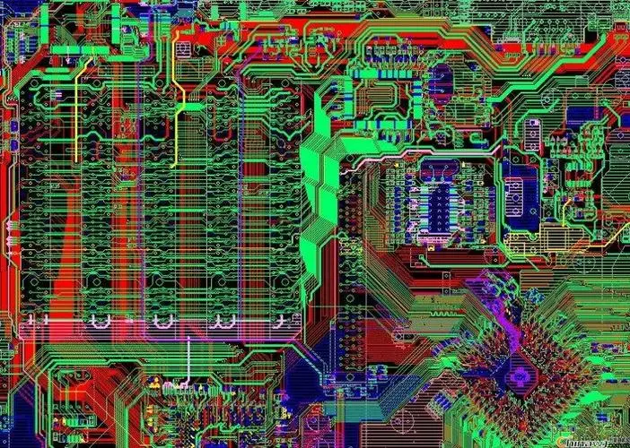
PCB refers to laying the road of power on signal to connect various PCB devices. In PCB design, wiring is an important step to complete product design. What are the common rules for PCB wiring?
1. Direction control rules for routing
During PCB wiring, the routing directions of adjacent layers are orthogonal, so as to avoid routing different signal lines in the same direction in adjacent layers, so as to reduce unnecessary inter layer interference. When it is difficult to avoid parallel wiring in PCB wiring, it should be considered to use ground plane to isolate each wiring layer and ground wire to isolate each signal line.

2. Open loop inspection rules for routing
In PCB wiring, in order to avoid the "antenna effect" generated by wiring and reduce unnecessary interference radiation and reception, it is generally not allowed to have a floating wiring form at one end.
3. Routing length control rules
The wiring length shall be as short as possible during design to reduce the interference problem caused by too long wiring. For driving multiple devices, the network topology should be determined according to the specific situation.
4. Impedance matching check rules
The wiring width of the same network shall be consistent. The change of the line width will cause the nonuniform characteristic impedance of the line, and reflection will occur when the transmission speed is high. Under some conditions, it may be impossible to avoid the change of line width, and the effective length of the inconsistent part in the middle should be minimized.
5. Chamfer rules
During PCB wiring, the corners of routing turns shall not be designed into acute angles and right angles to avoid unnecessary radiation; It is required that the included angle between all lines should be greater than or equal to 135 °. In the case that right angle corners are really needed for wiring, two improvement methods can be adopted: first, turn 90 ° corners into two 45 ° corners; Second, round corners are used
6. Device decoupling rules
Add the necessary decoupling capacitor on the PCB printed board to filter the interference signal on the power supply to stabilize the power supply signal.
7. 3W rule
In order to reduce the crosstalk between lines, ensure that the line spacing is large enough. When the line center spacing is not less than 3 times the line width, 70% of the electric fields can be kept from interfering with each other, which is called the 3W rule.
8. Ground wire loop rules
The minimum rule of the loop is that the loop area formed by the signal line and its loop should be as small as possible. The smaller the loop area is, the less external radiation is, and the less external interference is received.
9. Shielding protection
For some signals of special importance and high frequency, the copper shaft cable shielding structure design should be considered, that is, the wires laid on the line, below the line, left and right should be separated by ground wires, and how to effectively combine the shielding ground with the actual ground plane should also be considered.
10. Resonance rules of PCB wiring
Mainly for high-frequency signal design, that is, the PCB wiring length shall not be an integral multiple of its wavelength to avoid resonance.


Just upload Gerber files, BOM files and design files, and the KINGFORD team will provide a complete quotation within 24h.