
Professional PCB manufacturing and assembly
Building 6, Zone 3, Yuekang Road,Bao'an District, Shenzhen, China
+86-13410863085Mon.-Sat.08:00-20:00

How to move PCB signal for EMI
After helping customers to make their products meet EMI standards, a potential problem was found: poor PC board design Based on experience, designers of IoT products have encountered problems caused by poor people in PC board design When on-board energy destroys the sensitive receiver circuit, poor design may lead to infinite delay, which may lead to cellular compliance failure GPS and Wi Fi receivers will also lose sensitivity
How the signal passes through the PCB and how the movement of the electromagnetic field affects this movement The difference between good and bad PCB stacking
There are many factors that lead to poor EMI design. These include:
Use digital and sensitive analog circuits to mix noise circuits, such as power and motor switching.
Place the clock driver too close to the edge of the circuit board or too close to the sensitive circuit.
Bad routing that causes crosstalk.
Run the clock (or high-speed) track on the gap/slot that returns to the plane.
Most importantly, layer stacking errors.
Resolved the cross clock trace on the return plane gap. However, fixing the last item on layer overlays usually corrects numerous shortcomings, including many others on the list.
Circuit board

When taking college circuit courses, most of us were wrongly taught how DC and AC currents work in centralized or distributed (transmission line) circuits. In our "Field and Wave" course, we are unlikely to be guided in the practical application of circuit board design or the transmission of signals through circuit boards. In fact, when digital signal propagates through microstrip line or stripline, these two concept circuits and fields work together (complement each other).
Before you understand how signals are on PC boards, you must first understand some physics
We all know that "current" is the flowing copper of electrons. This is close to the fact, except that we tend to think that the positive current lacks electrons, which are usually called "holes". However, electrons and the "holes" they leave behind (positive charges) move very slowly.
Of course, this current is correct for the DC circuit (except for the initial battery connection transient). But for the "DC" output (with transient) of AC (or RF) circuits or switching power supplies, we need to understand that all connecting lines/wiring must now consider transmission lines.
Results First, let's consider how capacitors allow electrons to flow. After all, isn't that how decoupling capacitors work? If we add the battery to the capacitor, any positive charge applied to the top plate will repel the positive charge on the bottom plate, leaving a negative charge. If we apply alternating current to the capacitor, you may think that the current flows through the dielectric, which is impossible. James Clerk Maxwell called it "displacement current", in which positive charges only replace the positive charges on the opposite plate, leaving negative charges, and vice versa. The displacement current is defined as dE/dt (time-varying electric field).
The above is the explanation given by the editor of pcb circuit board company.
If you want to know more about PCBA, you can go to our company's home page to learn about it.
In addition, our company also sells various circuit boards,
High frequency circuit board and SMT chip are waiting for your presence again.
What rules should PCB thermal design follow?
Oct 22,2022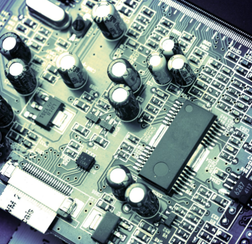


Just upload Gerber files, BOM files and design files, and the KINGFORD team will provide a complete quotation within 24h.