
Professional PCB manufacturing and assembly
Building 6, Zone 3, Yuekang Road,Bao'an District, Shenzhen, China
+86-13410863085Mon.-Sat.08:00-20:00

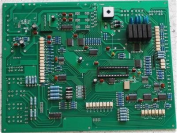
Multilayer PCB Routing Rules Summary
With the development of electronic technology, PCB technology is also progressing, and the requirements for wiring are also getting higher and higher. Reasonable wiring can ensure the performance and quality of the circuit board; But for single layer board and multilayer board, their routing rules are different. This article mainly summarizes the routing rules of multilayer PCB, and hopes to help you!
Multilayer PCB routing rules

1. Connect lines at more than 3 points, and try to let the lines pass through each point in turn, with the line length as short as possible.
2. The lines between different layers shall not be parallel as far as possible to avoid the formation of actual capacitance.
3. Try not to set out wires between pins, especially between and around integrated circuit pins.
4. The wiring shall be straight line or 45 degree broken line to avoid electromagnetic radiation.
5. The lines shall be as neat as possible, and the multiple paved lines shall be connected together as much as possible to increase the grounding area.
6. The elements shall be evenly arranged for installation, plug-in and welding.
7. The positive and negative electrodes of the SMD components shall be marked at the end of the package to avoid space conflict.
8. The function block components shall be placed together as much as possible.
9. The lead of high frequency circuit wiring should preferably be a straight line, which needs to be turned, and can be turned with a 45 degree broken line or an arc.
10. If the cabling space allows, insert a ground wire between two lines with serious crosstalk to reduce crosstalk.
11. If the wiring space permits, increase the spacing between adjacent signal lines, reduce the parallel length of signal lines, and try to make the clock line perpendicular to key signal lines.
12. After wiring, carefully check whether each connecting line is really connected.
The above is the explanation given by the editor of pcb circuit board company. If you want to know more about PCBA, you can go to our company's home page to learn about it. In addition, our company also sells various circuit boards,
High frequency circuit board and SMT chip are waiting for your presence again.


Just upload Gerber files, BOM files and design files, and the KINGFORD team will provide a complete quotation within 24h.