
Professional PCB manufacturing and assembly
Building 6, Zone 3, Yuekang Road,Bao'an District, Shenzhen, China
+86-13410863085Mon.-Sat.08:00-20:00

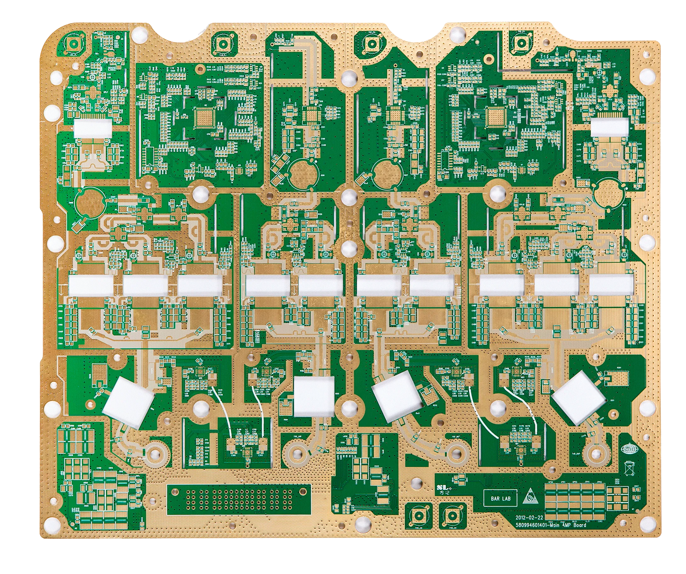
Printed circuit boards (PCBs) are required for most electronic devices, including smartphones, TVs, appliances, and more. Composite circuit boards are laminate structures of conductive insulating layers that serve two distinct functions: to place electronic components in designated areas of the outer layers and to provide reliable electrical connections between component terminals and conductive pads.

These electronic components (resistors, capacitors, microcontrollers, interfaces, etc.) are connected through traces, planes, and other features using a chemical etching process that laminates layers of copper to thin sheets of non-conductive substrates.
PCB Evolution
PCBs were developed in the early 20th century, and while they have continued to evolve with the advent of new technologies, their basic design has remained largely the same - a rigid board that houses electronic components.
Advances and widespread adoption of PCB technology have kept pace with rapid advances in semiconductor packaging technology, enabling industry professionals to develop smaller, more efficient electronic products. It has led to the development of wearable technologies such as AR/VR glasses, smart watches, and even interactable clothing.It’s also ushering in an era of body-worn medical devices capable of monitoring the wearer’s health through direct contact with skin and smartphones using technologies like folding displays. To realize these devices, a new type of PCB needs to be developed that can stretch and bend beyond right angles. The engineering community is making flexible PCB using a variety of technologies and materials, including polyimide, clear polyester, and more

1. Ultra-thin, flexible circuits make many applications practical.
Types of Flexible PCBs
Manufacturers use two types of malleable boards for today's devices: flex and rigid-flex PCBs. Flexible PCBs or FCBs function similarly to their rigid counterparts, where electronics are placed on a flexible substrate rather than a rigid platform. This enables different shapes and configurations to be formed. Depending on the layer and configuration, these can be divided into the two most common types mentioned earlier.
Rigid-flex PCBs are hybrid circuit boards that have both rigid and flexible sections to accommodate SMD (surface mount devices, also known as electronic devices) and connector arrangements. In this configuration, the SMD is mounted on a flexible substrate and the connector is on a rigid substrate to maintain a stable connection and mitigate damage from repeated use. The rigid-flex configuration also allows for increased productivity of the SMD since the connection terminals are placed on a rigid surface.
High-density interconnect (HDI) PCBs have higher routing densities than their rigid counterparts and offer finer lines and spaces, smaller vias and capture pads, and higher connection pad densities. These PCBs are beneficial when used with flexible substrates because they can take advantage of thinner layers or, in some cases, eliminate the need for multiple layers in the PCB design.The classification of FCB can be subdivided by the number of layers. For example, single-layer boards are made using a single polyimide substrate and thin copper layers that can be accessed from one side of the board. There are also single-sided FCBs with dual channels, double-sided FCBs with conductive copper on both sides of the substrate, and multi-layer FCBs with multi- and single-sided channel capabilities.
Flexible PCB Design
There are many questions that arise when designing a flexible PCB, the most important of which is how many times it will bend and to what extent. The number of times it can bend determines whether the board is static or dynamic.
2. Different materials will provide increased or decreased flexibility levels and represent their operating environment. (Source: Miraco on Wikipedia)
Static plates are considered bent installations and will be bent less than 100 times during their service life. Dynamic board designs need to be more robust because flexing occurs on a regular basis and may need to withstand tens of thousands of flexes depending on the application. Of course, the bend radius (the minimum curvature of the bend area) also comes into play and must be properly determined early in the design. This ensures that the design can withstand the necessary amount of bending without damaging the copper.Masks and other materials that cover the conductive layers of the FCB, as well as stiffeners to support different parts of the circuit, must also be considered during the design phase, which can be used on both sides of the board. It is important to note that the number of stiffeners applied will increase the stiffness of the design and reduce bending in some or all areas.
Like traditional PCBs, FCBs have a layered design, so the materials used must also be considered during the design phase. For example, a thin film layer provides a conductor carrier and acts as an insulator in a circuit, but it must also be flexible. Polyimide and PET (polyester) work well as insulators and are often used for these types of substrates. PEN (polyethylene phthalate), PTFE and aramid are also used.Polyimide flexible cores are also suitable for FCB designs. They are coated with electrodeposited or rolled annealed copper and are ultra-thin for both dynamic and static applications.FCB utilizes two types of materials: adhesive-based, where the copper is bonded to the polyimide with an acrylic adhesive; and adhesive-free, where the copper is cast directly onto the polyimide substrate. Of course, adhesive materials also have their drawbacks, including the formation of cracks when exposed to heat. They also make copper laminates thicker and tend to absorb moisture, which affects their use in certain environments.
This is where adhesive-free materials come into play. They can handle harsh environments and offer other benefits including reduced bend thickness, increased flexibility and better temperature ratings.
Flexible PCB stack
A PCB stack is the arrangement of copper and insulator layers that make up a PCB before designing the final layout of the board. While a stack-up layer allows you to assemble multiple electronic circuits on a single board through its various layers, the structure of a PCB stack-up design offers many other advantages, including reduced external noise, improved electromagnetic compatibility, and lower manufacturing costs. Using multiple layers increases the power distribution capability of the board, reduces cross-interference, eliminates electromagnetic interference, and supports high-speed signals.

3. A single-layer flex PCB stack-up looks a lot like a traditional PCB stack-up, but the material layers are different.
Like traditional PCBs, FCBs can be designed with one or more layers and represent the number of copper traces, adhesive, laminate, and polyimide material. These numbers depend on the number of layers. For example, a four-layer circuit would have four copper traces, four layers of adhesive (or non-adhesive), a laminate, and the corresponding substrate material. Many manufacturers will place flexible materials in the center of the stack to maintain flexibility and mitigate any damage during operation.When deciding on the number of layers, several factors must be considered before proceeding with the design, including the number of circuit signals that need to be routed, the frequency of operation, whether additional shielding is required, and other metrics. These will help represent the exact number of layers required and ensure that the FCB is functioning as expected.
In conclusion
Flexible printed circuit boards will continue to evolve as new technologies emerge. Imagine being able to clean medical monitoring equipment in a laundry room or wear a biometric patch while diving in the ocean without worrying about corrosion.
Devices that rely on flexible electronics can already capture data from the human body, so it will be interesting to see where this technology will be implemented. It is also important to note that this is only a basic introduction to flex PCB design, providing an overview of the materials and processes used to create them.
Analysis of flexible PCB technology
Printed circuit boards (PCBs) are required for most electronic devices, including smartphones, TVs, appliances, and more. Composite circuit boards are laminate structures of conductive insulating layers that serve two distinct functions: to place electronic components in designated areas of the outer layers and to provide reliable electrical connections between component terminals and conductive pads.These electronic components (resistors, capacitors, microcontrollers, interfaces, etc.) are connected through traces, planes, and other features using a chemical etching process that laminates layers of copper to thin sheets of non-conductive substrates.
PCB Evolution
PCBs were developed in the early 20th century, and while they have continued to evolve with the advent of new technologies, their basic design has remained largely the same - a rigid board that houses electronic components.Advances and widespread adoption of PCB technology have kept pace with rapid advances in semiconductor packaging technology, enabling industry professionals to develop smaller, more efficient electronic products. It has led to the development of wearable technologies such as AR/VR glasses, smart watches, and even interactable clothing.It’s also ushering in an era of body-worn medical devices capable of monitoring the wearer’s health through direct contact with skin and smartphones using technologies like folding displays. To realize these devices, a new type of PCB needs to be developed that can stretch and bend beyond right angles. The engineering community is making flexible PCB using a variety of technologies and materials, including polyimide, clear polyester, and more
1. Ultra-thin, flexible circuits make many applications practical.
Types of Flexible PCBs
Manufacturers use two types of malleable boards for today's devices: flex and rigid-flex PCBs. Flexible PCBs or FCBs function similarly to their rigid counterparts, where electronics are placed on a flexible substrate rather than a rigid platform. This enables different shapes and configurations to be formed. Depending on the layer and configuration, these can be divided into the two most common types mentioned earlier.
Rigid-flex PCBs are hybrid circuit boards that have both rigid and flexible sections to accommodate SMD (surface mount devices, also known as electronic devices) and connector arrangements. In this configuration, the SMD is mounted on a flexible substrate and the connector is on a rigid substrate to maintain a stable connection and mitigate damage from repeated use. The rigid-flex configuration also allows for increased productivity of the SMD since the connection terminals are placed on a rigid surface.
High-density interconnect (HDI) PCBs have higher routing densities than their rigid counterparts and offer finer lines and spaces, smaller vias and capture pads, and higher connection pad densities. These PCBs are beneficial when used with flexible substrates because they can take advantage of thinner layers or, in some cases, eliminate the need for multiple layers in the PCB design.The classification of FCB can be subdivided by the number of layers. For example, single-layer boards are made using a single polyimide substrate and thin copper layers that can be accessed from one side of the board. There are also single-sided FCBs with dual channels, double-sided FCBs with conductive copper on both sides of the substrate, and multi-layer FCBs with multi- and single-sided channel capabilities.
Flexible PCB Design
There are many questions that arise when designing a flexible PCB, the most important of which is how many times it will bend and to what extent. The number of times it can bend determines whether the board is static or dynamic.
2. Different materials will provide increased or decreased flexibility levels and represent their operating environment. (Source: Miraco on Wikipedia)
Static plates are considered bent installations and will be bent less than 100 times during their service life. Dynamic board designs need to be more robust because flexing occurs on a regular basis and may need to withstand tens of thousands of flexes depending on the application. Of course, the bend radius (the minimum curvature of the bend area) also comes into play and must be properly determined early in the design. This ensures that the design can withstand the necessary amount of bending without damaging the copper.
welding
Masks and other materials that cover the conductive layers of the FCB, as well as stiffeners to support different parts of the circuit, must also be considered during the design phase, which can be used on both sides of the board. It is important to note that the number of stiffeners applied will increase the stiffness of the design and reduce bending in some or all areas.
Like traditional PCBs, FCBs have a layered design, so the materials used must also be considered during the design phase. For example, a thin film layer provides a conductor carrier and acts as an insulator in a circuit, but it must also be flexible. Polyimide and PET (polyester) work well as insulators and are often used for these types of substrates. PEN (polyethylene phthalate), PTFE and aramid are also used.
Polyimide flexible cores are also suitable for FCB designs. They are coated with electrodeposited or rolled annealed copper and are ultra-thin for both dynamic and static applications.FCB utilizes two types of materials: adhesive-based, where the copper is bonded to the polyimide with an acrylic adhesive; and adhesive-free, where the copper is cast directly onto the polyimide substrate. Of course, adhesive materials also have their drawbacks, including the formation of cracks when exposed to heat. They also make copper laminates thicker and tend to absorb moisture, which affects their use in certain environments.This is where adhesive-free materials come into play. They can handle harsh environments and offer other benefits including reduced bend thickness, increased flexibility and better temperature ratings.
Flexible PCB stack
A PCB stack is the arrangement of copper and insulator layers that make up a PCB before designing the final layout of the board. While a stack-up layer allows you to assemble multiple electronic circuits on a single board through its various layers, the structure of a PCB stack-up design offers many other advantages, including reduced external noise, improved electromagnetic compatibility, and lower manufacturing costs. Using multiple layers increases the power distribution capability of the board, reduces cross-interference, eliminates electromagnetic interference, and supports high-speed signals.
3. A single-layer flex PCB stack-up looks a lot like a traditional PCB stack-up, but the material layers are different.
Like traditional PCBs, FCBs can be designed with one or more layers and represent the number of copper traces, adhesive, laminate, and polyimide material. These numbers depend on the number of layers. For example, a four-layer circuit would have four copper traces, four layers of adhesive (or non-adhesive), a laminate, and the corresponding substrate material. Many manufacturers will place flexible materials in the center of the stack to maintain flexibility and mitigate any damage during operation.When deciding on the number of layers, several factors must be considered before proceeding with the design, including the number of circuit signals that need to be routed, the frequency of operation, whether additional shielding is required, and other metrics. These will help represent the exact number of layers required and ensure that the FCB is functioning as expected.
In conclusion
Flexible printed circuit boards will continue to evolve as new technologies emerge. Imagine being able to clean medical monitoring equipment in a laundry room or wear a biometric patch while diving in the ocean without worrying about corrosion.Devices that rely on flexible electronics can already capture data from the human body, so it will be interesting to see where this technology will be implemented. It is also important to note that this is only a basic introduction to flex PCB design, providing an overview of the materials and processes used to create them.


Just upload Gerber files, BOM files and design files, and the KINGFORD team will provide a complete quotation within 24h.