
Professional PCB manufacturing and assembly
Building 6, Zone 3, Yuekang Road,Bao'an District, Shenzhen, China
+86-13410863085Mon.-Sat.08:00-20:00

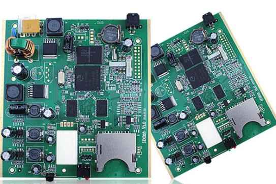
Rf and microwave pcba processing with high frequency laminates can be difficult to design due to signal sensitivity, especially compared to other digital signals.
Here are some things to consider to ensure that your design is efficient and minimizes the risk of malfunctions, signal interruptions, and other intrusions.
· RF and microwave signals are very sensitive to noise -- much more sensitive than ultra-high speed digital signals. This means that you need to work hard to keep noise, ringing, and reflection to a minimum, while carefully handling the overall system.
· The return signal takes the path with the least inductance -- the ground beneath the signal will ensure this path more easily.
· Impedance matching is important. As RF and microwave frequencies increase, the tolerance becomes smaller. Typically, your PCB driver needs to be fixed, such as 50 ohms, which means that during transmission and sending to the receiver, the driver outputs 50 ohms.
· Transmission lines that are bent due to wiring limitations should use a bending radius at least three times larger than the width of the center conductor. This minimizes the characteristic impedance.
· Return loss must be minimized, whether it is caused by signal reflection or ringing. The return path will always be found, but your design should guide it and prevent the return from bleeding through the many layers made by the pcba.
Use high frequency laminates
The laminated materials used to manufacture RF printed circuit boards add a layer of safety and protection to all of your equipment. These materials can help your device perform all three common types of heat transfer: conduction, convection, and radiation.
Thermal management is a top priority for all PCB applications in any industry, especially when high frequencies are used.
Finding the right high frequency laminate for your pcba manufacturer requires discovering a wide range of characteristics and determining how to combine them into one picture. This is a complex conundrum where you must make trade-offs between multiple options and use cases.
You should choose your high frequency PCB laminates based on how well they match your application, paying particular attention to some important features:
Coefficient of thermal expansion (CTE)
· Dielectric constant (Dk) and its heat coefficient
· Smoother copper/material surface profile
· Thermal conductivity
· Thickness
· Flexibility of conformal circuits

2. What are the technical indicators of dry film in the circuit board?
In order to better select and use dry film, smt patch manufacturers need to understand the technical performance and indicators of dry film and its technology. Generally, the following technical requirements for dry film should be understood.
(1) Appearance quality
Patch processing plant through the eye inspection, the appearance of dry film should be uniform, transparent, no fluid glue, no bubbles, no foreign impurities, no scratches and wrinkles on the surface. The use of dry film with these defects can cause quality problems or unuse of the mask. In the dry film into a roll, the winding should be tight, the edge is neat, in order to facilitate continuous film operation on the film machine.
(2) The thickness of dry film resist layer should be selected according to the purpose of use
If the corrosion resistance layer is used for etching, the thickness should be 25 ~ 30μm; If used for corrosion resistance of graphic electroplating, the thickness should be 38 ~ 50μm; If used as a mask resist, the thickness should be 25 ~ 50μm. The thinner the anticorrosive film for making ultra-fine printed wire graphics, the better, the higher the accuracy of the graphics, generally the thickness of the anticorrosive layer in the dry film is only ten microns.
As can be seen from the table, the thickness of products from different pcba manufacturers with similar uses varies. In application, dry film with appropriate thickness should be selected according to the needs and product instructions of specific patch processing plants. The width of the dry film can be cut according to the applicable requirements, the length of each roll is generally not less than 100m.
(3) The laminating process is usually in the laminating machine hot press roll temperature of 105℃±10℃, line pressure of 0. 54kgf/ cm and transmission speed of 0. 9 ~ 1. 8m/ min, the dry film can be firmly pasted on the substrate covered with copper foil.
(4) Spectral characteristics In the dry film, the spectral absorption wavelength of photoresist ranges from 310 nm to 420nm, and the wavelength of the safe optical region is greater than or equal to 460nm. High pressure mercury lamp and halide lamp can be used as light source for dry film exposure because of the high radiation intensity near ultraviolet region and most wavelengths in the spectral absorption region of photoresist. The main radiation energy of low pressure sodium lamp is in the wavelength range of 589.0 ~ 589.0 nm, and the monochromatic property is good, which conforms to the operation safety light of dry film, and the yellow light emitted is more sensitive to human eyes, bright, easy to operate.
(5) The sensitivity of dry film includes sensitivity speed, exposure time tolerance and depth exposure.
Shenzhen patch processing kingford today to take you to understand here, if you need to pay more attention to please contact us.

EMC layout design of PCB
May 23,2023


Just upload Gerber files, BOM files and design files, and the KINGFORD team will provide a complete quotation within 24h.