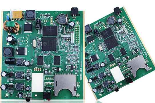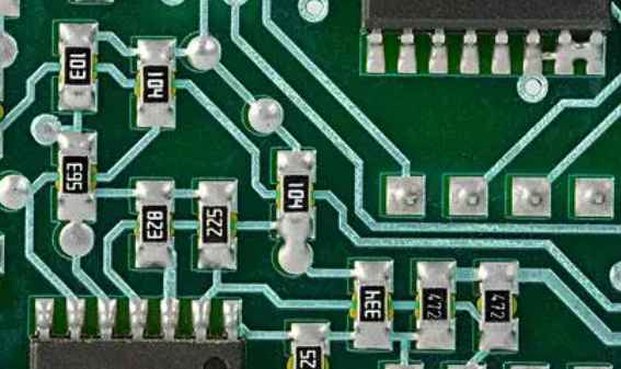
Improper layout of components on printed circuit board is an important factor that causes interference, so we should consider the circuit structure and arrange the components on the board reasonably. First of all, the size and shape of the printed circuit board should be determined according to the layout of the components. Large size will make the printed wire longer, increase impedance, reduce noise tolerance; Too small size is not conducive to heat dissipation, adjacent wires and devices are easy to induction.
In the layout of components on the board, in principle, the input and output parts should be arranged at the two extremes of the board; The interrelated components in the circuit should be as close as possible to shorten the distance between the connecting wires; Components whose working frequencies are close to each other or whose working levels differ greatly should be far away from each other to avoid mutual interference. For example, in the design and drawing of the printed circuit board of the commonly used microcontroller as the core of the small development system circuit, it is appropriate to place the clock generator, oscillator and other noise-generating devices close to each other, and keep the relevant logic circuit part away as far as possible. At the same time, considering the installation of the printed circuit board in the cabinet, it is best to arrange the ROM, RAM, power output device and power supply and other heat-prone components on the edge of the board or above the part, in order to facilitate heat dissipation.
In the layout of logic circuit on the board, in principle, high speed circuit should be placed near the output end, such as photoelectric isolator, and low speed circuit and memory should be placed slightly away, so as to deal with the problems of common impedance coupling, radiation and crosstalk. A buffer is placed at the input and output end for signal transmission between plates, which can effectively prevent noise interference.
In electronic equipment, digital circuit, analog circuit and power circuit components layout and wiring characteristics are different, they produce interference and interference suppression methods are different.
In addition, because of the different frequencies of high-frequency and low-frequency circuits, their interference and interference suppression methods are also different.
Therefore, in the component layout, the digital circuit, analog circuit and power circuit should be placed separately, the high-frequency circuit and the low-frequency circuit separated.
Conditions should be made separately isolated or separate into a circuit board. In addition, special attention should be paid to the distribution of strong and weak signals and signal transmission direction.
When high-voltage and high-power components are installed on the board, keep a certain distance between them and low-voltage and low-power components.
When placing high -, medium - and low-speed logic circuits on a printed board, the components should be arranged in the manner shown below.
Similar to other logic circuits, the components should be placed as close as possible to each other, so that better anti-noise effect and signal integrity can be obtained. EMC and SI problems should be fully considered in the placement of components on PCB.
One principle is to keep the leads between the components as short as possible. In terms of layout, it is necessary to separate analog signal part, high-speed digital circuit part and noise source part (such as relay, high-current switch, etc.) reasonably so as to minimize signal coupling between each other, as shown in the figure above.
Clock generator, crystal oscillator and CPU clock input are easy to produce noise, should be closer to each other. Devices, small current circuits and large current circuits that are easy to generate noise should be kept away from logic circuits as far as possible. If possible, it is important to make a separate circuit board. 2.1 Principles of special component placement

(1) Shorten the connection between high-frequency components as far as possible, and try to reduce their distribution parameters and electromagnetic interference between each other. Easily disturbed components should not be too close to each other, input and output components should be as far away as possible.
(2) There may be a high potential difference between some components or wires. The distance between them should be increased to avoid accidental short circuit caused by discharge. Components with high voltage should be arranged as far as possible in places that are not easily touched by the hand during debugging.
(3) Components weighing more than 15g shall be fixed with supports and then welded. Those large and heavy, heat components, should not be installed on the printed board, but should be installed on the chassis bottom, and should consider the problem of heat dissipation. Heat sensitive components should be far away from high power, high current and other heating components.
2 Function Partition
(1) Arrange the position of each functional circuit unit according to the flow direction of the circuit, so that the layout is convenient for signal flow, and keep the signal as consistent as possible.
(2) Take the core component of each functional circuit as the center, and carry out the layout around it. The components should be arranged evenly, neatly and compact on the PCB to minimize and shorten the leads and connections between the components.
3 General layout requirements for PCB components
Circuit elements and signal paths must be arranged to minimize coupling of unwanted signals:
(1) Low electronic signal channels should not be near high level signal channels and unfiltered power lines, including circuits that can generate transient processes.
(2) Separate the low level analog circuit from the digital circuit to avoid the common impedance coupling between the analog circuit, the digital circuit and the common circuit of the power supply.
(3) High, medium and low speed logic circuits should be used in different areas on the PCB.
(4) Minimize the length of signal line.
(5) Ensure that there are no long parallel signal lines between adjacent boards, between adjacent layers of the same board and between adjacent wiring on the same level.
(6) Electromagnetic interference (EMI) filters should be placed as close to the EMI source as possible and on the same circuit board.
(7) DC/DC converters, switching components and rectifiers should be placed as close as possible to the transformer to minimize its wire length.
(8) Place the voltage regulator and filter capacitor as close to the rectifier diode as possible.
(9) The printed board is divided according to the frequency and current switching characteristics, and the noise element and the non-noise element should be further away.
(10) The wiring sensitive to noise should not be parallel to the high-current and high-speed switching lines.


