
Professional PCB manufacturing and assembly
Building 6, Zone 3, Yuekang Road,Bao'an District, Shenzhen, China
+86-13410863085Mon.-Sat.08:00-20:00


Even an ordinary PCB can play a very important role in one-off development. The PCB is the physical platform on which the design takes place, and it is also the most flexible component used in the original component for electronic system design. Pater Technology often refers to these golden rules in the design process of PCB production.
This article introduces several golden rules of PCB design, most of which have not changed since the inception of commercial PCB design 25 years ago, and which are widely applicable to all kinds of PCB design projects. They are of great guidance to both young electronic design engineers and more mature circuit board manufacturers.
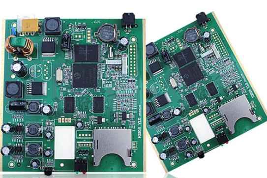
PCB design
The following article describes the ten most effective design principles that electronic design engineers should keep in mind and practice when using design software for PCB layout design and commercial manufacturing. Engineers do not need to implement these rules in order of time or relative importance; simply following them all can dramatically change product design.
Rule 1: Choose the right grid
Set and always use the grid spacing that matches the most components. While multiple grids seem to be effective, a little more thought early on in PCB layout can help engineers avoid spacers and get the most out of the board. Since many devices come in multiple package sizes, engineers should use the product that is best for their own design.
In addition, polygons are very important for copper coating of circuit boards. Polygon filling deviation in polygonal copper coating of multi-grid circuit boards is generally not as standard as that based on a single grid, but can provide board life beyond the required.
Rule two: Keep the path shortest and most direct

This may sound simple, but it should be kept in mind at every stage, even if it means changing the layout of the board to optimize the length of the wiring. This applies especially to analog and high-speed digital circuits where system performance is always limited in part by impedance and parasitic effects.
Rule 3: Use the power layer to manage the distribution of power cables and ground cables
Power layer copper is a faster and easier option for most PCB design software. By sharing a large number of wires, maximum efficient current with minimum impedance or voltage drop is guaranteed, while providing an adequate grounding return path.
If possible, multiple power supply lines can be run in the same area of the circuit board to verify that the ground layer covers most of a layer of the PCB, which facilitates the interaction between running lines on adjacent layers.
Rule 4: Group related components together with desired test points
For example, the discrete components required for an OpAmp are placed close to the device so that the bypass capacitors and resistors can cooperate with them, helping to optimize the length of the wiring mentioned in Rule 2, while also making testing and fault detection easier.
Rule 5: PCB assembly is performed by duplicating the required circuit board several times on another larger circuit board
Choosing the size that best fits the equipment used by the manufacturer helps reduce prototyping and manufacturing costs.
First lay out the board on the panel, contact the board manufacturer to get their preferred size specifications for each panel, then modify your design specifications and try to repeat your design several times within those panel sizes.
Rule 6: Integrate component values
As a designer, you choose discrete components that are either high or low in value, but equally efficient. By consolidating within a smaller range of standard values, bills of materials can be simplified and potentially cost reduced. If you have a range of PCBS based on preferred component values, it will be easier to make the right inventory management decisions in the long run.
Rule 7: Perform Design Rule Checks (DRC) as often as possible
Although it takes a very short time to run DRC functionality on PCB software, in more complex design environments, you can save a lot of time as long as you keep checking throughout the design process, which is a good habit to keep. Every wiring decision is critical, and DRC can remind you of the most important wiring decisions at any time.
Rule 8: Use screen printing flexibly
Screen printing can be used to label useful information for future use by circuit board makers, service or test engineers, installers, or equipment debuggers. Not only clearly indicate the function and test point labels, but also indicate the component and connector orientation as much as possible, even if these annotations are printed on the surface below the component used by the board (after the board is assembled).
The full application of screen printing technology on the upper and lower surfaces of the circuit board can reduce duplication of work and streamline the production process.
Rule 9: Decoupling capacitor is required
Don't try to optimize your design by avoiding decoupling power lines and basing it on limits in the component data sheet. Capacitors are cheap and durable, and you can take as much time as possible to assemble them, while following Rule six and using a standard range of values to keep your inventory in order.


Just upload Gerber files, BOM files and design files, and the KINGFORD team will provide a complete quotation within 24h.