
Professional PCB manufacturing and assembly
Building 6, Zone 3, Yuekang Road,Bao'an District, Shenzhen, China
+86-13410863085Mon.-Sat.08:00-20:00


First, PCB design of printed circuit board structure size design requirements
1. The size of the board must be controlled between 100-400mm in length and 80-220mm in width. Too large is not easy to control the deformation of the board.
2. On the premise of satisfying spatial layout and circuit, strive for simple shape rules. It is best to make a rectangle with a not too wide aspect ratio, and the best aspect ratio reference is 3:2 or 4:3.
3. The two long edges of PCB should be parallel, and the non-parallel edges should be added to facilitate the equipment transmission in the production and processing process.
4. Considering the efficiency of machine insertion and the needs of wave soldering comprehensively, if the long side of the main IC is parallel to the long side of the PCB, it is recommended to adopt a 4-piece design; if the long side of the main IC is perpendicular to the long side of the PCB, it is recommended to adopt a 3-piece design. When necessary, it is also recommended to adopt split-board machine insertion design to improve production efficiency.
5, printed circuit board
There should be positioning holes for testing tools, the diameter of positioning holes should be φ4.0+0.05/-0mm holes, hole distance tolerance requirements within ±0.08mm, the number of at least 3, should be placed as far as possible, and distance from the edge of the plate at least 2mm spacing, to ensure the production of the clockwise bed, testing tools, etc., convenient.
6. The structure size of the printed circuit board (including appearance and hole position) should be fully matched with the mechanical structure design of the electric control box. There should be no copper foil (except the required grounding) or components within the radius of the screw hole 3.5MM (or according to the requirements of the structure drawing).
7. The positioning size of the printed circuit board of the automatic plug-in process should meet the process requirements of the automatic plug-in machine. The allowable size of the PCB of the global automatic plug-in machine is mm*mm, and the allowable size of the PCB of the Panasonic automatic plug-in machine is mm*mm.
8. The positioning size of the printed circuit board of the automatic SMT process should meet the process requirements of the automatic SMT machine. The minimum allowable size of the PCB of the JUKE2050/2060 automatic SMT machine is (X) 50mm* (Y) 30mm, and the maximum size is (X) 410mm* (Y) 360mm.
9. On the PCB board with patches, in order to improve the accuracy of mounting the patch components, two MarkS points are generally required to be placed at the diagonal end of the patch layer. For example, a group of MarkS of the same form can be placed at the limited position. Mark the welding pad or through hole with a diameter of 1mm-1.5mm (1.5mm is preferred), and a circle with a diameter of 4mm shall be left outside the marking point. The circle range in the form of a solid circle shall be an open welding area or pattern, and the circle range in the form of a through hole shall be fully exposed to copper;
The MarkS reference point should be at least 5.0mm away from the PCB edge;
For IC(QFP) etc. When the pin spacing is less than 0.8mm, two marks are required to be added diagonally on the unit of the part as the correction mark of the part.
Two, the welding direction of the circuit board structure design requirements
1. In general, the direction of wave soldering on the printed circuit board should be parallel to the long side of the printed circuit board and perpendicular to the short side of the printed circuit board;
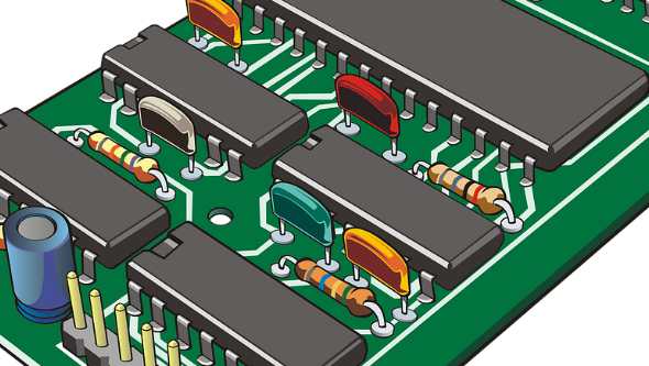
2. The direction of the crest should be consistent with the long side direction of the IC with close spacing of the component feet and the long side direction of the connector line, etc.; See the picture below.

3, PCB over the crest direction should be on the component surface of the screen layer with a clear, clear arrow mark;
PCB design pad design standard
First, PCB design
Design standard for shape and size of middle pads
▪ Should call the PCB standard package library.
▪ The minimum single side of all pads shall be no less than 0.25mm, and the maximum diameter of the whole pad shall be no more than 3 times of the component aperture.
▪ Try to ensure that the spacing between the edges of the two pads is greater than 0.4mm.
In the case of dense wiring, it is recommended to use oval and oblong connecting disks. The diameter or minimum width of single panel pad is 1.6mm; Double panel of weak current line welding pad only need to add 0.5mm hole diameter can be, welding pad is too large easy to cause unnecessary welding.
▪ Pads with aperture exceeding 1.2mm or pad diameter exceeding 3.0mm should be designed as diamond or plum pads
▪ For plug-in components, in order to avoid breaking of copper foil during welding, single-sided connection plates should be fully covered with copper foil; The minimum requirements of the double panel should fill tears; As shown below:
▪ All organic inserts should be designed as drip pads along the elbow to ensure full solder joints.
▪ The welding pad on the large area of copper skin should be chrysanthemum-shaped, without virtual welding. If the PCB has a large area of ground and power line (area over 500 square mm), it should be partially windowed or designed as a mesh FILL. As shown below:


Just upload Gerber files, BOM files and design files, and the KINGFORD team will provide a complete quotation within 24h.