
Professional PCB manufacturing and assembly
Building 6, Zone 3, Yuekang Road,Bao'an District, Shenzhen, China
+86-13410863085Mon.-Sat.08:00-20:00

First, the structure of the printed circuit board size
1. The size of the board must be controlled between 100-400mm in length and 80-220mm in width. Too large is not easy to control the deformation of the board.
2. On the premise of satisfying spatial layout and circuit, strive for simple shape rules. It is best to make a rectangle with a not too wide aspect ratio, and the best aspect ratio reference is 3:2 or 4:3.
3. The two long edges of PCB should be parallel, and the non-parallel edges should be added to facilitate the equipment transmission in the production and processing process.
4. Considering the efficiency of machine insertion and the needs of wave soldering comprehensively, if the long side of the main IC is parallel to the long side of the PCB, it is recommended to adopt a 4-piece design; if the long side of the main IC is perpendicular to the long side of the PCB, it is recommended to adopt a 3-piece design. When necessary, it is also recommended to adopt split-board machine insertion design to improve production efficiency.

5, printed circuit board
There should be positioning holes for testing tools, the diameter of positioning holes should be φ4.0+0.05/-0mm holes, hole distance tolerance requirements within ±0.08mm, the number of at least 3, should be placed as far as possible, and distance from the edge of the plate at least 2mm spacing, to ensure the production of the clockwise bed, testing tools, etc., convenient.
6. The structure size of the printed circuit board (including appearance and hole position) should be fully matched with the mechanical structure design of the electric control box. There should be no copper foil (except the required grounding) or components within the radius of the screw hole 3.5MM (or according to the requirements of the structure drawing).
7. The positioning size of the printed circuit board of the automatic plug-in process should meet the process requirements of the automatic plug-in machine. The allowable size of the PCB of the global automatic plug-in machine is mm*mm, and the allowable size of the PCB of the Panasonic automatic plug-in machine is mm*mm.
8. The positioning size of the printed circuit board of the automatic SMT process should meet the process requirements of the automatic SMT machine. The minimum allowable size of the PCB of the JUKE2050/2060 automatic SMT machine is (X) 50mm* (Y) 30mm, and the maximum size is (X) 410mm* (Y) 360mm.
9. On the PCB board with patches, in order to improve the accuracy of mounting the patch components, two MarkS points are generally required to be placed at the diagonal end of the patch layer. For example, a group of MarkS of the same form can be placed at the limited position. Mark the welding pad or through hole with a diameter of 1mm-1.5mm (1.5mm is preferred), and a circle with a diameter of 4mm shall be left outside the marking point. The circle range in the form of a solid circle shall be an open welding area or pattern, and the circle range in the form of a through hole shall be fully exposed to copper;
The MarkS reference point should be at least 5.0mm away from the PCB edge;
For IC(QFP), when the pin spacing is less than 0.8mm, two marks are required to be added on the diagonal of the unit of the part as the correction mark of the part, as shown in the figure below:
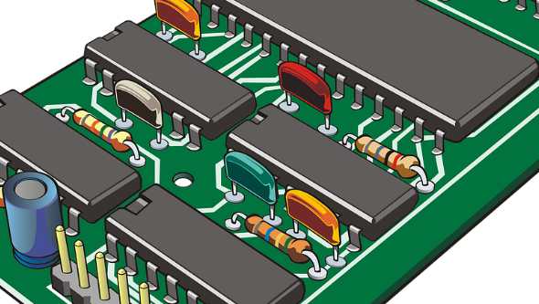
Two, welding direction
1. In general, the direction of wave soldering on the printed circuit board should be parallel to the long side of the printed circuit board and perpendicular to the short side of the printed circuit board; See the picture below.
2. The direction of the crest should be consistent with the long side direction of the IC with close spacing of the component feet and the long side direction of the connector line, etc.; See the picture below.
3, PCB over the crest direction should be on the component surface of the screen layer with a clear, clear arrow mark; See the picture below.
Three, device layout
1. Requirements for device layout of process equipment
Component layout should be neat and beautiful, the same type of components should be integrated
▪ Based on the direction of over-wave soldering (reflow soldering) of PCB, the spacing between the front and rear plates of any component or its body should be more than 4.0mm, and the spacing between the left and right plates should be more than 5.0mm; Otherwise, a process edge must be added. To facilitate processing and transportation.
▪ The layout of printed circuit boards using automatic plug-in technology should meet the technical requirements of automatic plug-in machines.
2, the placement of components should consider the height of components, component layout should be uniform, compact, beautiful, balanced center of gravity, and must ensure installation.
▪ The location of components should be at the grid points recommended by the circuit design software (2.54mm).
▪ The spacing between any component body should be at least 0.5mm, at least not close together. To prevent the component is difficult to plug in place or unfavorable heat dissipation.
▪ Considering the convenience of assembly, production line maintenance and after-sales service maintenance, the socket design of external parts is easy to plug in the position, the selection of the socket and the color of the socket can be distinguished to ensure that there will be no mistakes in plugging.
▪ Component layout should be matched with electric control box assembly. Tall components, especially pin relay, fan capacitor, strong electric socket, high-power raising resistance, mutual inductance, etc. should have a gap between the highest point and the box body after assembly into the electric control box, so as to affect the smooth assembly and stress, resulting in reduced reliability of electric control.


Just upload Gerber files, BOM files and design files, and the KINGFORD team will provide a complete quotation within 24h.