
Professional PCB manufacturing and assembly
Building 6, Zone 3, Yuekang Road,Bao'an District, Shenzhen, China
+86-13410863085Mon.-Sat.08:00-20:00

Without effective communication and communication between project PCB designers, multiple different versions of PCB design data may be generated, and there may be a lot of design duplication among team members. If different versions of design data cannot share a unified standard and format, it will inevitably cause communication barriers and management difficulties among members. Repetitive design and effort will inevitably reduce the efficiency of the entire team.
If you can't anticipate these problems in advance and take steps to avoid them, it often takes more time and effort to resolve them when conflicts arise later in the design. In this way, although the overall team operation affects efficiency, it may also affect the development cycle and budget of the project.
The question now before us is: how can we preserve the design results that have been validated as successful and reuse the design for future designs or other team members to avoid duplicate designs? How to design multiple circuits with the same circuit structure cleverly? How can each member of the team collaborate fully and use the same standards and templates to manage data? How can team managers fully understand and control the big picture?
Design code segments (code segments)
As a diligent and conscientious electronic engineer, you must have designed many circuits in your PCB design career. It must have accumulated a lot of successful PCB design modules and been proven. Some of these successful designs may be reused in other similar products or projects in the same line. Including its schematic diagram and PCB. Is there an easy way to save these design parts and reuse them easily in other PCB designs without having to do the same job over and over again? Or do other colleagues on the same team need to use this part of the design instead of designing from scratch and just copy and paste the saved design results?
Altium Designer offers just such a feature, namely Design Fragments (Snnipet). Save the design pieces in a folder, and then copy the ready-made schematic design and PCB design pieces into your own project as easily as you copy the pieces. The advantage of this approach is that in addition to easily copying an off-the-shelf design, you can also make your own tweaks and changes to the copied design pieces. For example, make some changes to some wiring, replace some parts, etc.
The reuse of design fragments is the unique strength of Altium Designer's unified design platform. If you are in a multi-clock design software exchange design environment, a simple fragment copy approach will not work because the design data follows a different structure.
Equipment list
In terms of module reuse, is there a way to take my frequently used circuit diagrams as a whole and call them around like components? Can it be called by different designers on different projects?
Don't worry, the Altium Designer equipment sheet is just for that! The software comes with many, many mature design modules. The schematics of these design modules are made into device tables that you can call as a component.
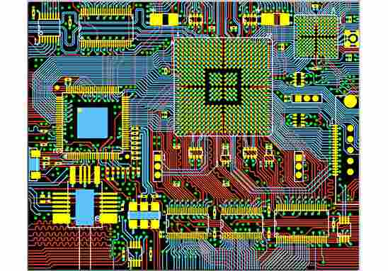
The FLASH_S29GL256N11FFIV10_16Mx16 has been made into a device table. (The green block diagram is in the upper right corner. Multiple projects, such as using components, then invoke this device type diagram (placing it on top of the diagram and compiling a subdiagram of this device table for display). The two different design items of this device table are called NB2DSK. PRJPCB and daughter board. PRJPCB. This makes it easy for different members of the team to reuse the same schematic module. Just save it as a device table and call it at will.
For device-based schematics, in addition to the rich and varied device tables provided by the software itself, engineers themselves can make device-based schematics using their own works or design modules, which may be reused in the future. Save it in the location you specify for easy recall or sharing with others as needed.

Multi-channel design method (multi-channel)
In PCB design, it is often necessary to reuse the same schematic diagram in different locations. For example, a high pressure common rail electronic fuel injection system or an electronic fuel injector in the Marine industry requires the same drive circuit (same circuit structure and components) as a 6-way fuel injection system to maintain drive consistency. Or a centralized control unit has exactly the same control circuit for multiple control terminals. In this case, we don't need to copy and paste the same copy schematic for each channel.
Because this copying and pasting is relatively clear in the schematic, it is a mess at the PCB layout stage, and there is no guarantee that every channel has the same layout structure and wiring. These small differences can also affect execution or timing issues. 16 channels of the exact same circuit, fed into the PCB, completely destroyed the components, how do I find them one by one and put them where they should be? It's too much trouble!
Therefore, this multi-channel design (using the same schematic repeatedly) must ensure that the schematic is clear and easy to understand and that the layout and wiring on the PCB are exactly the same. Let's take a look at how Alitum Designer can use multi-channel design to simplify the engineer's workload.
For example, the schematic should be reused five times, i.e., five channels. Then first generate the top block diagram of the 5 channels and repeat the 5 layers overlay.
Import data from the schematic to the PCB. Five rooms will be generated, and five schematic circuit frames will be placed in five different rooms. Place and arrange one of the channels. The fan-shaped rooms at the top have been laid out and mapped out.
Then use the Copy Room Format feature to convert the 5 rooms to the exact same layout and sector structure. Then the layout and wiring of these 5 channels are put together according to the circular polar coordinates to form a circle. This approach ensures great convenience in the PCB layout and wiring phases, and is error-free.
Various design templates maintain standard consistency (templates)
1. Schematic diagram template
If the circuit diagram of a PCB design project is more complex and larger, it is often not possible to stack all designs on the same schematic diagram. The circuit will be divided into several sub-circuit modules, each sub-circuit module will be marked with the corresponding title bar, common functions, etc. Generally speaking, in order to complete and beautiful design, when others read your electroplating drawing, they can understand the overall basic situation of the circuit at a glance from your drawing title bar and the connection structure of related modules. Therefore, the title bar and author information on each schematic, especially when different designers design drawings, must have a uniform standard for the title bar and related information, so as not to be caused by a variety of styles. However, in the context of such large-scale projects and teamwork, the design and application of schematic templates is particularly demanding.
Because it is a military agency, the title bar contains, in addition to general and commonly used information, special requirements such as names, materials, confidentiality levels, as well as hierarchical approval and filing procedures for design, proofreading, review, standard inspection and verification. Finally, for the uniformity of design, the same title bar is designed for different paper sizes to facilitate the management and archiving of design data.
2. PCB design template
In PCB design, if the size, interface layout and installation positioning holes of multiple boards in the same series of products have been determined to remain unchanged, PCB templates need to be made. Every time a new design is done, the schematic will be imported directly into the PCB design template, saving a lot of board design, peripheral layout design, and installation and positioning part of the design. Apply the energy directly to the design change itself. Greatly save unnecessary duplication of labor, and no error.
3. BOM template
Information construction has become the only way for modern enterprises to rapidly enhance their core competitiveness and realize leapfrog development. Nowadays, enterprises no longer pursue the informatization of single point and partial application, but pay more and more attention to the overall informatization of application integration, process optimization and information sharing.
In enterprises, BOM (BOM) runs through the whole ecological process of product conceptual design, detailed design, process planning, prototype trial production, manufacturing, sales and maintenance, as well as the end of the product. With the continuous advancement of enterprise information construction, BOM has become the core of enterprise product data management and the foundation and bridge of data integration among various application information systems. BOM management has become the main content of enterprise engineering informatization and management informatization.
In lifecycle management, the BOM runs through the beginning and end of the lifecycle. From the provision of BOM, BOM management, to the use of BOM are inseparable. At Altium Designer, BOM also runs through the entire process from concept design of electronic products to final manufacturing, sales and maintenance.
Altium Designer offers circuit design Boms that can be imported into structural step parts and can be changed and managed during the design process. After the design is completed, the information of process BOM, purchase BOM, manufacture BOM and assembly BOM will be displayed during the processing and manufacturing of electronic products, procurement BOM, manufacturing BOM and assembly BOM. It plays an important role in the whole product life cycle.
Therefore, the BOM template is also very rich.
Altium Designer's BOM template data source can collect a full range of information, with N types of output templates (for purchasing, manufacturing, assembly, audit, etc.). File formats are also rich and varied.
For each BOM template file, which columns need to be captured and which contents can be configured and modified by yourself. You can locate the source BOM template file (located in the Template folder of the installation directory) to configure the captured data columns. Finally, output the BOM information to meet the different purposes you need.


Just upload Gerber files, BOM files and design files, and the KINGFORD team will provide a complete quotation within 24h.